
New in Altium Designer
This page details the improvements included in releases of Altium Designer, Altium Designer Develop and Altium Designer Agile. Along with delivering a range of improvements that develop and mature the existing technologies, each update also incorporates a number of fixes and enhancements across the software based on feedback raised by customers through the AltiumLive Community's BugCrunch system, helping you continue to create cutting-edge electronics technology.
Version 26.1
Altium Designer Develop – Released: 3 December 2025 – Version 26.1.0 (build 6)
Altium Designer Agile – Released: 3 December 2025 – Version 26.1.0 (build 13)
Altium Designer – Released: 3 December 2025 – Version 26.1.0 (build 7)
Release Notes for Altium Designer
PCB Design Improvement
Solder Mask Expansion Rule Default Now 0 Mils (Open Beta)
Observing the IPC-7351B standard in relation to padstack defaults, where the solder mask openings are typically a 1:1 ratio of the land size, the values for the Solder Mask Expansion rule (in PCB documents) and rule-driven solder mask expansion (in PCB library documents) are now set to 0 mil by default (previously 4 mil).
For a PCB library (*.PcbLib), support for these new default values are at the library level, inherited by all component footprints created therein. The same PCBlib will show, for all object rule-driven solder mask expansion, 4 mils expansion when opened in a previous version of Altium Designer and 0 mils expansion when opened in this release and later, as shown below for a pad object.

For a PCB document (*.PcbDoc), all existing Solder Mask Expansion rules store their initial values. The default values used for any newly created rule are determined by the version of Altium Designer where that rule was created and will not change while opening in another version of Altium Designer. Therefore, the default is 4 mils expansion when created in a previous version of Altium Designer and opened in any other version, and 0 mils expansion when created in this release (or later) and opened in any other version, as shown below.

A newly created Solder Mask Expansion design rule in the Constraint Manager.

A newly created Solder Mask Expansion design rule in the PCB Rules and Constraints Editor dialog.
For more information about the Solder Mask Expansion design rule, refer to the Mask Rule Types page.
Constraint Manager Improvement
Added Ability to Filter Classes
An ability to filter classes has been implemented in the Constraint Manager's Clearances view to leverage your work with a large number of classes. This enables the construction of filters (or groupings) of classes to allow switching between, and working with, focused sub-sets of the clearances matrix.
Use the ![]() button at the top right of the Clearances view to access a pop-up from where you can create, edit, remove, and enable/disable filters.
button at the top right of the Clearances view to access a pop-up from where you can create, edit, remove, and enable/disable filters.
![]()
To create a new filter, click the ![]() button and then click the
button and then click the ![]() button in the pop-up that appears.
button in the pop-up that appears.
![]()
Define a unique name for the new filter, enable the required group of classes, and click ![]() .
.
![]()
With a filter created, use the available controls in the pop-up to enable, disable, edit, or remove it as needed. Note that when a filter is enabled, the button at the top right is shown as ![]() .
.
For more information about working with the clearance matrix, refer to the Defining Design Requirements Using the Constraint Manager page.
Draftsman Improvement
Enhanced DXF Import to Draftsman Documents (Open Beta)
This feature adds support for importing DXF files version R12 and later into manufacturing drawing documents (*.PCBDwf, *.HarDwf, *.MbDwf). Importing DXF files including splines is also now supported.
For more information about importing DXF files, refer to the Draftsman Placement & Editing Techniques page.
Wire Bonding Improvement
Bond Wire Primitives in Panels
Bond wires are now presented with the correct type (Bond Wire) in the following places:
-
The Primitives region of the PCB panel, with a selected component in Nets mode
-
The Component Primitives region of the PCB panel, with a selected net in Components mode
-
The PCB Library panel, with a selected footprint.
Selecting a bond wire primitive will select/highlight that bond wire within the design space.


In addition, a corresponding Show Bond Wires option is now available on a region's right-click context menu, for toggling bond wire visibility.
For more information about wire bonding, refer to the Wire Bonding page.
3D-MID Design Improvement
3D-MID Design Rule Check (Open Beta)
This release provides batch Design Rule Checking (DRC) for Width, Clearance, Length and Matched Lengths rule violations, in respect to routed tracks on your 3D substrate. Note that while a generated DRC report will provide information for all of these checks, only clearance violations will be highlighted within the design space.


For more information, refer to the 3D-MID Design page.
Multi-board Design Improvement
Ability to Define 'Termination Type' for Harness Entries
The Termination Type for a harness entry can now be defined on a multi-board schematic. The termination types available are:
-
Connector – the standard option used when connecting to a mating connector on the PCB. It typically involves standard board-mounted connectors.
-
Crimps/Ferrules – individual wires are terminated with crimps or ferrules before being inserted into the connector on the PCB side.
-
Wire termination – wires are blunt-cut at the harness end and either screwed down or soldered directly to the PCB. This is common with direct wire-to-board connections such as with some JST connectors.
The information is reflected in the properties for the selected harness entry and the corresponding module entry.


For more information about working with connections on a multi-board schematic, refer to the Working with Connections page.
Harness Design Improvements
Enhanced Synchronization of Wires
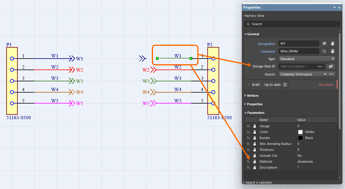
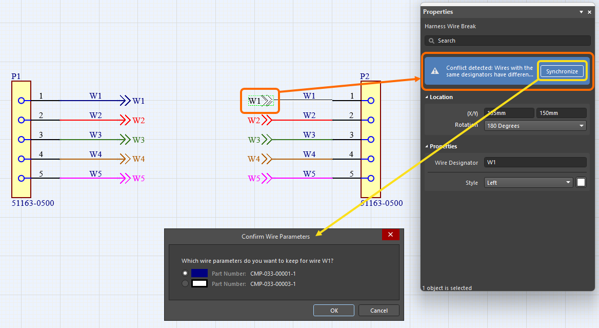
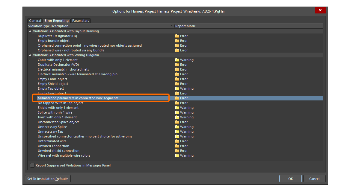
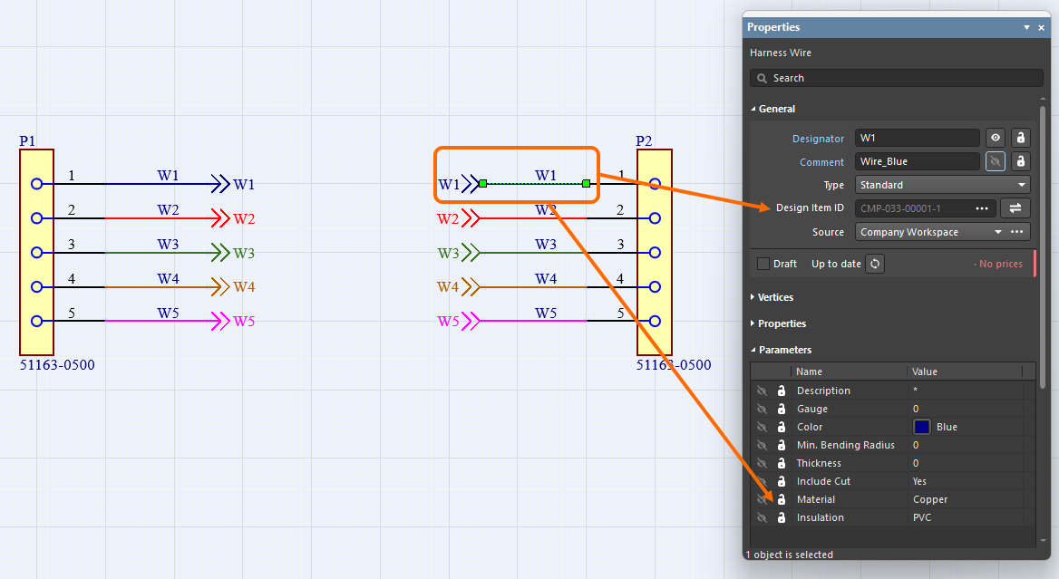
Harness wires connected with a wire break are now recognized even if they have different Design Item IDs. In addition, all wire segments with the same designator connected by the same wire break are now compared (for part number, comment, color, and all parameters). If any differences are found, the Mismatched parameters in connected wire segments violation is reported. A warning also appears in the Properties panel of the wire and wire break signifying that a conflict has been detected between the parameters. Click Synchronize within the warning to open the Conflict Wire Parameters dialog, which gives you the choice of which parameters to use for the wire segment.
Ability to Place a Covering over a Junction Point
You can now apply/extend a harness covering over a junction point (a connection point in the layout drawing where two or more bundles come together) on the harness layout drawing (*.LdrDoc). This removes the need to have separate harness coverings between junction points in a section that contains several connectors.

In addition, the start of a covering is now taken as the left-most, top-most point of its path, and that path now includes only the bundles the covering lays on.
For more information, refer to the Creating the Layout Drawing page.
Quantity Field in BOM Changed to 'As Required' for Certain Objects
Wire, cable, and harness coverings are length-based objects and the value is displayed in the Length field. To avoid confusion, the Quantity field for wire, cable and harness covering entries in a Bill Of Materials table and an ActiveBOM document in a manufacturing drawing document (*.HarDwf) is now As Required.

For more information, refer to the Managing Your Bill of Materials (BOM) with ActiveBOM page.
Improved Pin Grouping in Wiring List
Pin grouping in a wiring list that is placed in a harness manufacturing document (*.HarDwf) has been improved. Starting with this release, automatic grouping is applied to the connector with the most wires, and all of its cavities are correctly grouped in the From column of the wiring list as shown in the image below.

Excel Workbook for Harness Manufacturers
Added the ability to generate, through an Output Job, a single Excel Workbook containing data for use by harness manufacturers. To facilitate this, a new outputter – Manufacturing Data – is available under the Report Outputs section.

The generated Workbook includes four distinct sheets:
-
Bill of Materials – useful for quick quote generation.
-
Wiring List – for use with wire processing machines.
-
Labels – a summary of the physical labels to be printed for harness bundles, for use with Zebra or other printers.
-
Coverings – a summary of the coverings to be applied over harness bundles.


For more information, refer to the Preparing Reports page.
Platform Improvement
Switching to .NET 8
With this release, Altium Designer switches from using .NET 6 to .NET 8. This is bundled as a part of Altium Designer and enables it to take advantage of later functionality and developments with .NET, including general performance enhancements.
For more information, refer to the System Requirements page.
WebView2 (Open Beta)
Starting from this release, WebView2 is used for browser-related elements within Altium Designer (e.g., the Home page). This delivers access to the latest web browser engine within Altium Designer, just by updating Windows.
Data Management Improvements
Ability to Copy Workspace Project Using Process Workflow
Added support for making a copy of a Workspace project using defined (and enabled) process workflows. When a Workspace project is opened, right-click the project entry in the Projects panel and select an activated process definition (that is part of the Project Creations theme) from the Make a copy of the managed project sub-menu to start copying the project in accordance with the underlying workflow for that process.

For more information, refer to the Process-based Project Creation page.
Added Ability to Preserve Lifecycle State when Releasing Models
When releasing a new revision of a component model (schematic symbol, PCB footprint, simulation model, or harness wiring) to the connected Workspace, you can now preserve the model's current lifecycle state.

Note that this ability is available for those with assigned Allow to skip lifecycle state change for new revisions operational permission (learn more about Setting Global Operation Permissions for a Workspace).
For more information about editing Workspace content, refer to the Creating & Editing Content page.
Design Review Comment Links
When a comment is added as part of a design review, a link to that review (From <DesignReviewName>) is now presented within a corresponding entry in the Comments And Tasks panel and the contextual commenting window for that comment (within the design space). Click the link to open the review's Overview page in a new tab of your default browser.

For more information about document commenting, refer to the Document Commenting page.
Support for Additional Unit-aware Data Types
When defining a user parameter as part of a component template in a connected Workspace on the Altium Platform, the following additional unit-aware data types are now supported:
-
Area (mm2)
-
Bar (bar)
-
Bit
-
Candela (cd)
-
Decimal
-
Integer
-
Joule (J)
-
Lumen (lm)
-
Millimetre (mm)
-
Pascal (Pa)
-
Pounds per square inch (psi)
-
Rotations per minute (rpm)
-
Siemens (S)
-
Tesla (T)

Parameters using these new unit types are supported in various areas of the software, including the Components panel, the Component editor (in both single and batch editing modes), and by the Library Importer and Components Synchronization feature (in the Parameter Mapping section of the Properties panel).
For more information about the unit-aware component parameter data types, refer to the Component Templates page.
Ability to Sync Part Choices when Using Components Synchronization
The ability to define and sync part choice information using the Components Synchronization feature and its related Components Synchronization Configuration document (*.CmpSync) has been added. Control of the synchronized parameters is available in the Part Choices Mapping region of the Properties panel when a table is selected in the document. Use the buttons to add and remove part choice parameter pairs (Manufacturer / Part Number) and drop-down menu options to define the mapping. When mappings are defined, the corresponding parameters appear under Part Choice n columns in the document grid area.

For more information about the Components Synchronization feature, refer to the Component Database to Workspace Data Synchronization page.
New Warning Regarding Problems Connecting to a Workspace
If there is an issue connecting to a Workspace and the latest VCS states of project documents are not able to be refreshed, the Refresh VCS Statuses control (with associated tool-tip warning) now appears next to the project entry in the Projects panel. Once connection resumes, click the entry to bring the VCS states back into sync and to see the latest changes.

For more information about indicating document status, refer to the Managing Project Documents page.
BOM CoDesign Improvement
Excluding Supplier-related Fields from BOM Comparison Result (Open Beta)
When comparing an ActiveBOM with a selected Managed BOM by using the BOM CoDesign feature, when the advanced setting is disabled, supplier-related data (Supplier and Supplier Part Number parameters) is excluded from the Differences section on the Related BOMs tab of the Properties panel when it has been accessed from an ActiveBOM document.


For more information about exploring comparison results, refer to the BOM CoDesign page.
Import/Export Improvements
Enhanced Allegro Design Imports
All configuration files that are required are now included in the Allegro2Altium.bat file, a batch file included in your Altium Designer installation and used to convert an Allegro binary (*.brd or *.dra) file to ASCII format (when such a design/library is not on the same PC as Altium Designer). Therefore only the bat file is required for the import and no additional files.
For more information about exploring comparison results, refer to the Importing a Design from Allegro page.
Support for Component Alternative Views from xDX Designer Designs
Alternate view modes for components are now supported, in both generated schematic and schematic library documents, when importing an xDX Designer design.
For more information about exploring comparison results, refer to the Importing a Design from xDX Designer or DxDesigner page.
Features Made Fully Public in Altium Designer 26.1
The following features are now officially Public with this release:
-
Detailed Pad Stack for Allegro Imports - available since 25.7
-
Properties Panel Optimization for PCB Object Properties - available since 25.7
Additional Features in Altium Designer 26.1
-
Hidden Links to External VCS Repositories (Open Beta): A new advanced settings option –
VCS.HideProjectExternalRepositoriesLinks– is available in the Advanced Settings dialog with this release which, when enabled, hides links to external VCS repositories (created automatically when making a project under external VCS available to a connected Workspace) on the Data Management – Design Repositories page of the Preferences dialog ( ).
).
-
Simbeor Version (Open Beta): A new advanced settings option –
PCB.SimbeorVersion– is available in the Advanced Settings dialog with this release. This feature controls the version of Simbeor used in the calculation of delay and impedance (Simbeor 2020.3 (option '0') or Simbeor 2023.1 (option '1')). -
Via Instancing (Open Beta): A new advanced settings option –
PCB.ViaInstancing– is available in the Advanced Settings dialog with this release. When this option is enabled, the concept of 'via instancing' is utilized, an approach for building the geometry of an instance of a via, rather than a via template. This enhances performance while reducing both memory consumption and scene building time. -
Loading Optimization of Pad and Via Templates (Open Beta): A new advanced settings option –
PCB.Performance.PadViaTemplate.LoadingOptimization– is available in the Advanced Settings dialog with this release, which speeds up loading of PCBs by optimizing pad and via templates loading. -
ECO Processing Optimization (Open Beta): A new advanced settings option –
WSM.DotNetECOImplementation– is available in the Advanced Settings dialog with this release, which enables the use of accelerated ECO processing functionality.