Comparison of PCB Material Properties for High Speed Design and HDI Boards

Table of Contents
Any PCB uses a variety of materials to create a layer stack-up, etch copper, apply solder mask, and print silkscreen. Each dielectric material you use to create your multilayer PCB stack-up has different material properties, such as dielectric constant and thermal conductivity. When you’re designing for specialized applications, a thorough comparison of PCB material properties can help you select the right base material for use in your next circuit board. Altium Designer gives you the features you need to select a base material for your multilayer PCB and prepare your new design for full-scale manufacturing.
ALTIUM DESIGNER
The most powerful, modern, and easy-to-use PCB design tool for advanced electronics. Use any PCB material properties and prepare your board for manufacturing with Altium Designer.
Any PCB stack-up you create for your circuit board will include multiple materials. Many different materials will be used during PCB manufacturing. The materials you choose will determine power/signal loss, interconnect impedance, temperature rise, copper surface roughness, and temperature rise in your PCB. Not every base material is ideal for every application, so you’ll need to pick just the right base material for your PCB stack-up to balance performance in these different areas.
With a thorough comparison of PCB material properties, you can determine the best base material to use for your next system. Once you determine the best material to use for your circuit boards, the PCB stack-up design and analysis tools in Altium Designer help you create a PCB layout for high-speed circuit boards or HDI designs. Here is a comparison of PCB material properties to help you choose the right base material for your circuit boards.
Important Base PCB Material Properties
When selecting a base material for your PCB, you need to consider the various material properties of the material and how they fit into your board’s application. Here is the important PCB material for high-speed design properties you need to consider in your PCB:
- Relative Dielectric Constant: This is a complex number consisting of the relative permittivity (Dk) and dissipation factor (Df). The Df value is related to the loss of tangent in the material.
- Conductor Loss: Conductor losses come in AC and DC varieties, both of which are related to the electrical conductivity of your conductors. The electrical conductivity determines the skin depth, which determines AC losses. Note that conductor loss in copper on a PCB substrate is related to copper surface roughness, which will increase loss in the system and change the impedance of the interconnect.
- Thermal Conductivity: This determines the rate at which heat is dissipated away from the substrate during operation, and it determines the temperature rise with respect to ambient temperature. This will then determine your thermal management strategy, such as the use of a heat sink or fan to keep components cool.
- Coefficient of Thermal Expansion (CTE): This tells you how the board expands as its temperature increases. CTE is anisotropic, meaning the board will expand at different rates in different directions. Normally, we only care about expansion along the z-axis, i.e., perpendicular to the surface layer of a circuit board.
- Glass Transition Temperature (Tg): The glass transition temperature tells you when the CTE value suddenly increases as the temperature continues to increase. The CTE value above Tg is larger than the CTE value below Tg.
- Dispersion: The relative dielectric constant is a function of the signal’s frequency. Therefore, dispersion is not a specific number but is rather a property that defines how signals with different frequencies move with different propagation delay values in an interconnect.
Fabricators continue to discover materials better suited to high-speed circuit boards, HDI circuit boards, and high-temperature environments. The various material properties above affect how high-speed signals propagate in a substrate due to dispersion, as well as how they disperse heat and withstand mechanical shock. Some of these materials are suitable for microwave and mmWave devices, or for use in high-temperature environments, but they are more expensive to produce. Your best bet in choosing a material is to start with FR4 and evaluate whether this material will be suitable for your application.
Standard PCB Stackup Materials
The industry primarily uses grade FR4 nonconductive material between layers of copper to build printed circuit boards. FR4 is a NEMA-grade designation for glass-reinforced epoxy laminate material. The designation represents the ratio of fiber to resin and indicates characteristics such as flame retardant, dielectric constant, loss factor, tensile strength, shear strength, glass transition temperature, and z-axis expansion coefficient. FR4 is flame retardant making it suitable for safety requirements, and it is robust in varying temperature and humidity environments, increasing the quality of performance.

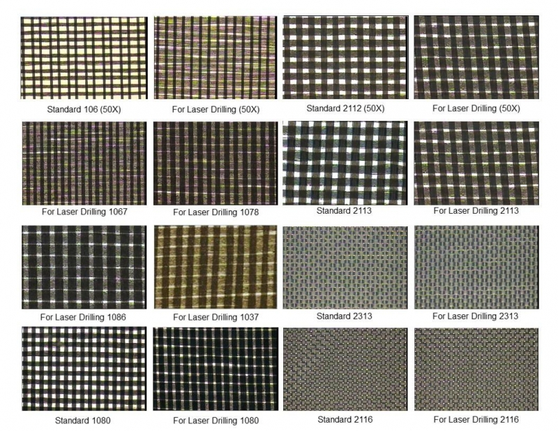
Standard fiberglass-impregnated resin laminates.
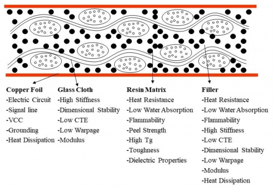
The major material components of PCBs are polymer resin (dielectric material) with or without fillers, reinforcement, and metal foil. To form a PCB, alternate layers of dielectric, with or without reinforcement, are stacked in between the copper foil layers. The majority of PCB material properties for high-speed design is epoxy, but some can be BT, PPE, cyanate ester, and modified acrylates. The structure of a typical epoxy PCB laminate is shown above.

Cross-section of a fiberglass-impregnated resin laminate.
These laminates are placed between layers of copper and become substrates with dielectric properties relevant to the circuits assembled onto the boards. Designers specify substrate thickness to meet dielectric requirements for the circuits. IPC-2221 contains tables specifying dielectric constant for FR4 and other laminate materials in PCB substrate layers. The best set of PCB design and layout tools will use this data to model impedance and loss in your PCB stack-up for optimal routing and trace design.
- Dispersion can be difficult to model if you are not familiar with high-frequency behavior in PCB dielectric materials.
Learn more about high-frequency dielectric dispersion in FR4 PCB material for high speed design.
- The surface roughness on a PCB laminate and copper surface roughness will affect the real and imaginary impedance of traces in your PCB.
Learn more about modeling copper surface roughness in your PCB.
- You can create your PCB stack-up with any dielectric material arrangement when you use the right set of PCB design tools.
Learn more about working with the Layer Stack Manager in Altium Designer.
PCB Material for High Speed Design and HDI
The backbone resin of the industry has been epoxy resin. Epoxy has been a staple due to its relatively low cost, strong adhesion (both to the metal foils and to itself), and desirable thermal, mechanical, and electrical properties. Basic epoxy chemistry has been dramatically changed over the years. Alternative resin-based PCB stack-up materials are typically selected to address specific shortcomings of epoxy-resin systems. BT-Epoxy is common for organic chip packages due to its thermal stability, while polyimide and cyanate ester resins are used for their lower Dk and Df values.
Besides thermosetting resins, thermoplastic resins are utilized including polyimide and polytetrafluoroethylene (PTFE). Unlike the thermoplastic version of polyimide which is relatively brittle, the thermosetting version is flexible and is supplied in film form. It is typically used to make flexible circuits as well as the combination circuits called rigid-flex. It is also more expensive than epoxy and is only used as needed. Many companies have gone to a “Halogen-Free” requirement in anticipation of an eventual ban on bromine-based flame retardants used in advanced PCB dielectric materials.
Such properties are ideal for high-speed and HDI PCBs. A lower dielectric constant allows signals in these boards to travel faster and lowers capacitive coupling between adjacent signal traces. This helps ensure signal integrity in these boards by reducing crosstalk between adjacent signal lines. This is especially important in HDI boards, where traces are packed into small spaces.
Alternative PCB Stackup Dielectric Options
If you’re designing for a high-temperature or high-power application, there are alternative substrate options available. These alternative substrates can also be used for HDI and high-speed PCB designs, giving you more flexibility to choose the best base material for your circuit board.
- Ceramic PCB substrate materials provide very high thermal conductivity and smoother dispersion at high frequencies, making them ideal for use in high-temperature environments.
- Metal-core PCB substrates are often used for single-layer or two-layer circuit boards that will run at high power and reach a high temperature.
- For a flex or rigid-flex PCB, you’ll need to choose a class of flexible materials with smooth copper foil on the surface layer.
Learn more about flexible base material options for flex and rigid-flex PCB design.

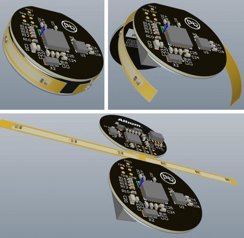
Rigid-flex PCB design is easy in Altium Designer.
Create Your PCB Stackup in Altium Designer
The Layer Stack Manager in Altium Designer includes a library of standard fiberglass weave materials with well-defined dielectric constant, CTE value, and dispersion models. If you are working with a more specialized material, such as RT Duroid or an aluminum core PCB, you can define dielectric constant and loss from a datasheet. You can then design controlled impedance traces with an integrated field solver. Everything you need to ensure signal integrity and route HDI boards is present in Altium Designer.
Altium Designer’s Draftsman tool provides information on copper and PCB stack-up dielectric material options required for PCB manufacturing. Materials for solder paste and hole plating are communicated as well. The use of RoHS materials is becoming the norm as the removal of lead solder and other toxic materials becomes mandatory worldwide.
Assembly instructions and fabrication details are enumerated on the general-purpose mechanical layers built into the layer stack. Special layers within the Layer Stack Manager are dedicated to specifying silkscreen, solder and paste mask, drill information, keep-outs, and interconnect layers.
The Unified PCB Design Environment in Altium Designer
The unified environment in Altium Designer also includes layout and routing features for creating high-speed PCBs, HDI circuit boards, and rigid-flex PCBs. Every function in Altium Designer is built on a rules-driven design engine, and all your PCB layout and routing tools are accessible within a single program. The simulation features in Altium Designer are also ideal for examining signal integrity in high-speed and HDI circuit board material properties.
- The design rules-driven engine in Altium Designer automatically flags errors as you create schematic drawings and your PCB layout. You can stay productive and design powerful electronics in this unique design environment.
Learn more about Altium Designer’s unified rules-driven design environment.
- To help ensure signal integrity in materials for HDI and high-speed circuit board material properties, Altium Designer includes an integrated 3D field solver for impedance and signal integrity calculations.
Learn more about Simberian’s 3D field solver in Altium Designer.
- If you’re new to integrated PCB design, Altium gives you access to PCB design tutorials and resources through Altium Academy.
Learn more about PCB material for high-speed design in Altium Designer through Altium Academy.

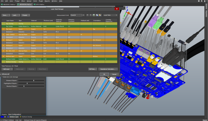
Create your PCB stack-up and specify the dielectric constant for your circuit boards in Altium Designer.
PCB material comparison chart for high-speed design and HDI circuit board material properties is a serious subject for PCB designers and electrical engineers. Several resources exist that provide a comparison of PCB board material properties, but you need design software that lets you use any material for PCB stack-up design. The PCB design features in Altium Designer let you select materials for your advanced PCB stack-up, and you’ll have access to a full suite of CAD features and simulation tools.
Altium Designer on Altium 365 delivers an unprecedented amount of integration to the electronics industry until now relegated to the world of software development, allowing designers to work from home and reach unprecedented levels of efficiency.
We have only scratched the surface of what is possible to do with Altium Designer on Altium 365. You can check the product page for a more in-depth feature description or one of the On-Demand Webinars.


