Altium Designer is Your Complete PCB Toolkit

Table of Contents
Designing a printed circuit board and its PCB assembly are intricate processes. If want to bring your next great electronic device to life, you’ll need to transform it from a circuit diagram into a schematic. Then you’ll need to turn your schematic into a layout and ensure it complies with DFM guidelines for your application. Different PCB tools in your design software can help with different tasks, but only one software package integrates all these features into a single interface. Altium Designer is the only PCB toolkit that gives you access to these features and much more.
ALTIUM DESIGNER
A fully unified PCB design package with a complete PCB toolkit and advanced design features.
Electronic design automation tools allow designers to route boards in a virtual environment before going into fabrication and assembly. This virtual environment is driven by schematic and layout editors to create a CAD document for your circuit board. Complex electronics need simulation features and control over design rules,
If you have access to a PCB toolkit with all these features, you can create a productive design workflow and examine all aspects of your circuit board functionality. Rather than using a software package that separates critical design features into separate programs, you need a software package that allows you to draw schematics, build your layout, plan for manufacturing, and manage your data all in one place. The new paradigm in PCB design software integrates these features into a single package, and all of these important features are present in a single interface.
Start With Your Schematic
Creating your schematic is the first step to breathing life into your new product, and it forms the foundation of all future work you will do to create your device. Most schematic editor software comes with some CAD capabilities and should read data directly from your component libraries. The best schematic editor should allow you to create hierarchical and multichannel schematics for complex products.

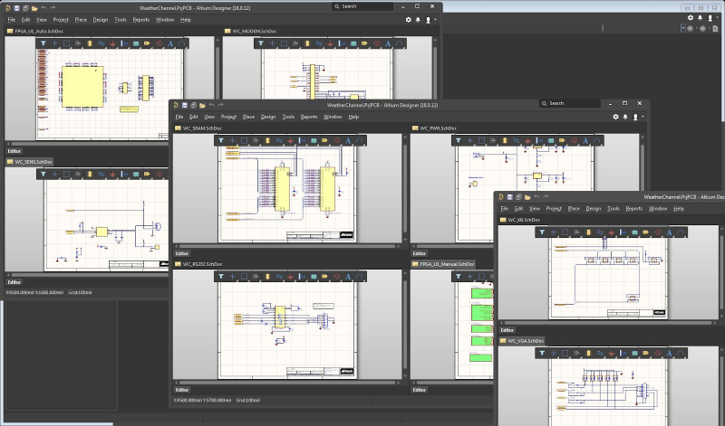
Hierarchical and multichannel schematic editor tool in Altium Designer’s PCB toolkit
The best schematic software gathers information directly from your component libraries and checks your design choices against standard and custom design rules. You can catch and correct any design mistakes before they compromise the functionality of your finished PCB. You can also segment groups of components into multiple schematics and link these schematics together into a single device using hierarchical design.
Build the Best Schematics With the Best PCB Design Tools
Unfortunately, most online or standalone PCB tools are only useful for drawing schematics. Once you’re ready to create an actual PCB layout, you need to use a schematic capture tool to import components into a blank circuit board. The best PCB toolkit will include schematic capture features alongside your schematic editor to start creating your new PCB layout.
- Any printed circuit board will start as a new schematic and will eventually turn into a circuit board layout with a schematic capture utility.
- Hierarchical schematic design helps you keep track of the links between different circuit blocks in complex devices.
Learn more about building PCBs with hierarchical schematics.
- Once you’ve finished designing your schematic, it’s time to start your PCB layout. You’ll need schematic capture to create an initial PCB layout.
Learn more about using your PCB design software for schematic capture.

The schematic editor in Altium Designer
Building Your PCB Layout From Your Schematic
A PCB layout is more than just a drawing of your components and connections placed on a circuit board. Your layout includes information on signal nets, differential pair routing, routing between layers with vias, and much more. Basic CAD tools that aren’t built for advanced design tasks don’t include this functionality. Instead, you need a complete PCB toolkit for basic and advanced design tasks.
Advanced electronics require strong routing tools that help you stay productive and cut down your PCB layout time. This type of PCB toolkit should include everything from fine-pitch BGA fanout and pin swapping features to CAD tools for accurately arranging components and defining rooms on your board. You can then verify signal integrity in your PCB layout with a post-layout simulation package in your PCB toolkit.
Prepare Your PCB Layout for Production
Instead of drawing out two versions of your PCB, your design software should include tools that capture your schematic as an initial layout. Instead of routing everything manually, you’ll want to use great PCB design software that includes automatic routing tools. When your design software is built on a single rules-based design engine, you can rest assured that your automated tools can properly route connections in your design while meeting basic and advanced design constraints.
Once you’ve finished your layout and schematic, it’s time to put together a comprehensive production plan. You’ll need to create a bills of materials, Gerber files, and other deliverables for your fabricator. Other PCB design programs force you to constantly move your design data between programs, which hampers your workflow and creates the potential for errors. Instead of sacrificing your productivity, you should invest in a PCB design platform that unifies your design tools.
- Your PCB tools should give you the freedom to implement any routing style in your circuit board as you create your PCB layout.
Learn more about routing styles in your printed circuit design and routing tools.
- The best PCB design software and routing features will check your layout against your design rules to ensure your circuit board will operate as designed.
- Modern PCB designs come with multiple layout challenges. When you have a dense board that is packed with advanced components, you need adaptable routing tools to overcome any design challenge.

Edit traces within routing environment
Bringing Your PCB Tools Together
Creating a PCB layout requires a complete PCB toolkit in a single program. Furthermore, you need design tools that access the same set of design rules for your application. Design rules are important for preventing mistakes when creating schematics and for your layout and routing PCB tools. You’ll need software that includes standard design rules for any PCB and allows you to customize new design rules for your application.
Only software with a powerful design rules engine can interface directly with the data in your components library, ensuring that your components are compatible with each other and your board performs as designed. This is the type of design environment you’ll find in Altium Designer, where multiple PCB tools work together in a single program. You can access all the features in a powerful PCB toolkit when you use Altium Designer.
Altium Designer Unifies Your PCB Design Process
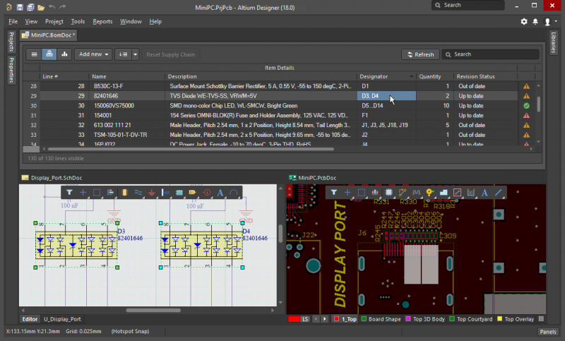
With the PCB toolkit in Altium Designer, you can begin your design in a schematic, create a complete PCB layout, and generate manufacturing documentation in a single program. Along the way, you can access pre-layout and post-layout simulation features to evaluate your board’s functionality and ensure your design will work as intended. The rules-driven design environment ensures your tools will work together and prevents data errors as you create your circuit board.
- Altium Designer gives you a complete PCB toolkit for schematic design, PCB layout and routing, and manufacturing preparation. The rules-driven design environment allows all tools to be accessed in a single program.
Learn more about the rules-driven design environment in Altium Designer.
- The Altium 365 platform allows you to backup, access, and share your Altium Designer data and components with other PCB designers. You’ll have a complete data management solution when you use Altium 365.
Learn more about managing and sharing your design data with Altium 365.
- If you want to learn more about using Altium Designer, you can access design tutorials and resources through Altium Academy.
Learn more about PCB design in Altium Designer through Altium Academy.

The CAD interface in Altium Designer
Altium Designer creates a complete PCB toolkit and analysis platform in a single program thanks to its unified environment and rules-driven design engine. Instead of working with separate design programs, try using the only complete PCB toolkit on the market. Invest in your success with Altium Designer.
Altium Designer on Altium 365 delivers an unprecedented amount of integration to the electronics industry until now relegated to the world of software development, allowing designers to work from home and reach unprecedented levels of efficiency.
We have only scratched the surface of what is possible to do with Altium Designer on Altium 365. You can check the product page for a more in-depth feature description or one of the On-Demand Webinars.


