
管脚面板
This document is no longer available beyond version 21. Information can now be found here: Edit Pin Mapping for version 24
Parent page: Working with Panels
Function
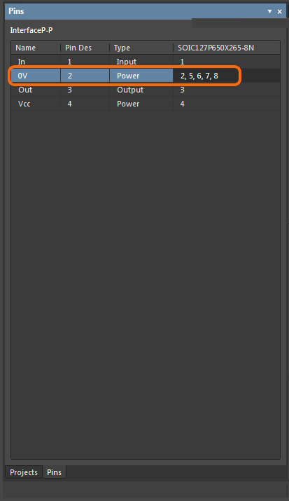
The Pins panel displays a pin mapping grid for the current component. The panel allows the default one-to-one pin-pad mapping to be changed to a custom relationship, such as one pin being connected to multiple footprint pads or any other non-aligned pin to pad number relationship. The panel allows you to define\edit and view mapping between pins and pads.
Panel Access
The Pins panel can be accessed from the Single Component Editor in the following ways:
- Click the Panels button at the bottom-right then select Pins from the pop-up menu.
- Click View » Panels » Pins.
- Click the
 icon near the top-right of the editor.
Content and Use
The panel displays a grid showing the pin mapping for the current component. When mapping a pin to multiple pads, the mapping entries are entered using a comma-delimited numeric format (1, 2, 3, 4, etc.). Pin-to-pad cross-probe highlighting is supported for multiple common footprint pads, and a custom footprint mapping configuration is indicated by its associated  icon.
icon.
A placed component with custom pin-to-pad mapping is fully supported during design schematic-PCB synchronization, for pin and part swapping, and by the Component Pin Editor dialog. Note that schematic components show pad designators rather than pin designators, and where custom mapping has been applied, the pin designator is displayed in gray. The latter can be disabled by unchecking the Show Pin Designators option on the Schematic - Graphical Editing page of the Preferences dialog.