添加过孔缝合和过孔屏蔽
Parent page: Finalizing the Board Design
Via stitching is a technique used to tie together larger copper areas on different layers, in effect creating a strong vertical connection through the board structure, helping maintain a low impedance and short return loops. Via stitching can also be used to tie areas of copper that might otherwise be isolated from their net, to that net.
Via shielding has a different function, in RF designs it is used to help reduce crosstalk and electromagnetic interference in a route that is carrying an RF signal. A via shield, also known as a via fence or a picket fence, is created by placing one or more rows of vias alongside the signal's route path. In Altium Designer, this is referred to as via shielding.
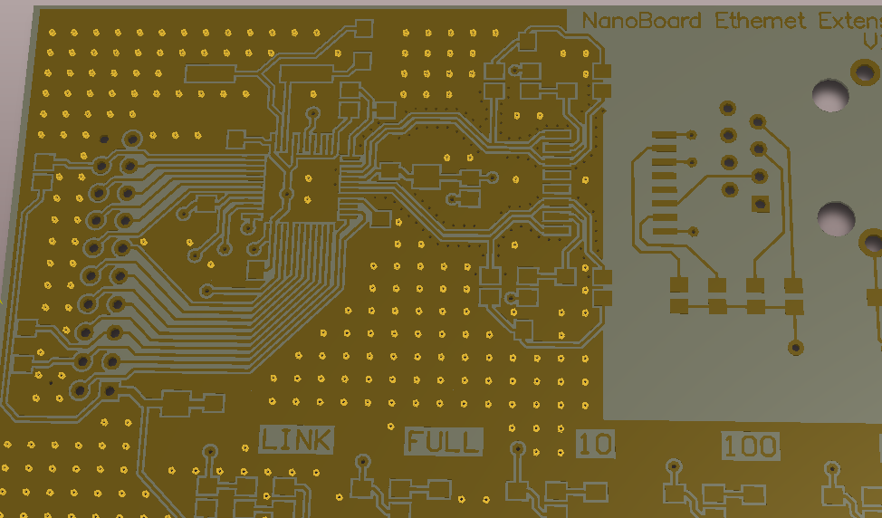
Altium Designer supports both via stitching and via shielding. In the image below, shielding vias are highlighted, move the cursor over the image to highlight the stitching vias that have been added to this board.
.") Use the Via Stitching and Via Shielding commands to stitch copper on different layers, and to add a wall of shielding vias adjacent to a route path (hover to highlight shielding vias).
Use the Via Stitching and Via Shielding commands to stitch copper on different layers, and to add a wall of shielding vias adjacent to a route path (hover to highlight shielding vias).
Let's look at stitching vias first, and then shielding vias.
Adding Stitching Vias
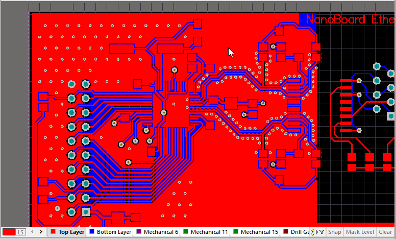
Via stitching is run as a post-process, filling free areas of copper with stitching vias. For via stitching to be possible, there must be overlapping regions of copper that are attached to the specified net, on different layers. Supported regions of copper include Fills, Polygons and Power Planes.
Select the Tools » Via Stitching/Shielding » Add Stitching to Net command from the menus to add stitching vias to a specific net. The Add Stitching to Net dialog will open, where the Stitching Parameters and Via Style are specified. Using the selected net, the stitching algorithm identifies all Fills, Polygons and Power Planes attached to that net and attempts to connect them through the board, using the specified via and stitching pattern.
The via stitching algorithm treats Polygons, Fills and Planes in the following way:
- Polygons and Fills that are on the same net are stitched wherever they overlap on different layers. If there are Polygons or Fills on other nets that are overlapping within that area (on another layer), stitching is not applied in that region. Overlapping Plane regions on other nets are passed through.
- Overlapping Plane regions on the target net are always stitched, regardless of the presence of Plane regions (on another layer) attached to other nets. Rule 1 above applies if there are Polygons or Fills overlapping in the same region.
Configuring the Stitching Parameters
Notes about the Add Stitching to Net dialog settings:
- Select the Net to be used for stitching first as this effects the behavior of other options, such as clicking the Load values from Routing Via Style Rule button. The Net dropdown is toward the bottom of the dialog, in the middle.
- The Grid is the distance between the centers of adjacent stitching vias, and applies in the X and Y directions. Stitching vias will not be placed in violation of applicable design rules, if a potential via site would result in a violation, that site is skipped.
- If the Stagger alternate rows option is enabled, alternate rows of stitching vias are offset by half of the Grid value.
- The Same Net Clearance options control the clearance between stitching vias, and vias and pads on the same net. There are two ways of controlling the clearance between same-net objects , either the applicable Clearance design rule is used, or the Default Via/Pad Clearance specified in the dialog is used. If an applicable rule exists, then the tighter of these two settings is used. Use the Create new clearance rule button to add a new Clearance design rule into the rules dialog, based on the settings you have entered in the Default Via/Pad Clearance field.
- The stitching Via Style can be configured manually, or it can be selected from those available in the Template dropdown, or it can be imported from the applicable Routing Via Style design rule by clicking the Load values from Routing Via Style Rule button. Clicking this button will load the Preferred rule settings.
Constraining the Via Stitching to an Area
As well as covering the entire board, stitching vias can be constrained to a user-defined area. When the stitching is within a user-defined area, that area of vias can be interactively moved and resized, if required.
 Enable the Constrain Area option to restrict stitching vias to a user-defined area.
To constrain via stitching to a specific area, enable the Constrain Area checkbox in the Add Stitching to Net dialog, as shown above. As soon as you enable this option the dialog will close and the cursor will change to a crosshair, ready to define the area - note the Status bar, it will prompt Select the first point of the area.
The process of defining a via stitching area is the same as defining a solid region or a polygon, you:
- click to define a series of vertices (corners),
- right-click to drop out of placement mode and automatically close and complete the area.
During placement there are a number of different corner modes available:
- press Shift+Spacebar to cycle through the corner modes (you might find the right-angle corner mode the most appropriate),
- press Spacebar to toggle the corner direction,
- press the 1 shortcut to toggle between placing 1 or 2 edges with each click.

 Press Shift+Spacebar to cycle corner modes, Spacebar to toggle the corner direction, 1 to toggle between placing 1 edge or 2 with each click.
Once the area is defined you will return to the Add Stitching to Net dialog, so you can configure the rest of the settings. Click OK when this is complete, Altium Designer will then analyze the area, identify potential via sites, and place the stitching vias.
Modifying a User-Defined Via Stitching Area
The set of vias in each unique area of via stitching are clustered into a Union (a set of objects that the PCB editor recognizes as a single group). The entire union can be moved, and the area can also be resized.
To modify via stitching that is constrained to an area:
- Drag a select-within rectangle (left-to-right) so that it includes one or more of the stitching vias. The boundary of the stitching area will be displayed, as shown in the animation below.
- To move a stitching union - position the cursor within the area, when the move cursor
 appears click and hold then move the area to the new location.
 - To resize the stitching union by moving an edge - position the cursor over the edge, when the move edge cursor
 appears click and hold then slide the
edge to the new location.
appears click and hold then slide the
edge to the new location. - To resize the stitching union by moving a vertex - position the cursor over the edge, when the move vertex cursor
 appears click and hold then slide
the vertex to the new location.
appears click and hold then slide
the vertex to the new location. - After you release the mouse button you will be prompted to Re-generate via stitching?, click Yes to update the via stitching in the new location/shape.
Drag a selection window to select a stitching area, then move or resize by positioning the mouse to get the correct cursor.
Adding Shielding Vias to a Net
To place a via shield around a routed net, select the Tools » Via Stitching/Shielding » Add Shielding to Net command from the menus. The Add Shielding to Net dialog will appear, configure the Shielding Parameters and Via Style as required. The vias will be placed along both sides of the chosen net, wherever it is possible to place a via that complies with the applicable design rules.
Configuring the Shielding Via Parameters
Notes about the Add Shielding to Net dialog, and using shielding vias:
- Select the Net to be shielded first as this effects the behavior of other options, such as clicking the Load values from Routing Via Style Rule button.
- If you do not want to shield the entire net, select the required track segments first, run the Add Shielding to Net command, then enable the Selected Objects option.
- To shield a differential pair, add shielding to each net in the pair.
- Use the Add shielding copper option to add a polygon that encloses the shielding vias, include the Add clearance cutout option to clip the polygon back to just enclose the vias. Read the Including Shielding Copper with the Stitching topic below to learn more about these options.
- The shielding Via Style can be configured manually, or it can be selected from those available in the Template dropdown, or it can be imported from the applicable Routing Via Style design rule by clicking the Load values from Routing Via Style Rule button. Clicking this button will load the Preferred rule settings.
- The size and positioning of the shielding vias is not an exact science, but there are guidelines that have been established based on empirical testing.
- As noted in the discussion forum(5) referenced below, for a PCB with an on-board antenna, "the distance between vias should be 1/4 your resonant wavelength at the most."
- The forum discussion also references a technical note(6), which states that "the common rule of thumb is to locate stitch vias no further apart than λ/10 and preferably as often as λ/20."
Including Shielding Copper with the Stitching
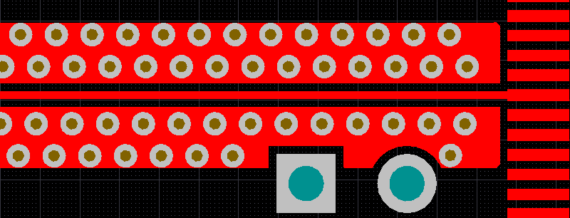
As well as adding shielding vias along each side of the routing, you can also include shielding copper, as shown in the image below. To do this, enable the Add shielding copper option. This copper is created as a polygon, so it obeys the applicable Clearance and Polygon Connect Style design rules.
The Add shielding copper option will add a polygon that encloses the shielding vias. The polygon edge that is away from the shielded net will touch the edge of the vias. The polygon edge that is adjacent to the shielded net will be set back from the net by the applicable Clearance design rule. If the Add clearance cutout option is also enabled, the polygon will instead be set back from the shielded net by the Distance setting in the Add Shielding to Net dialog. Hover the cursor over the image below to see the difference.
 Shielding vias around a net with the clearance cutout option enabled, move the cursor over the image to disable the clearance cutout option.
Identifying Vias that are Part of a Stitching or Shielding Array
Each via in a stitching or shielding array is identified by the addition of of a string to the net name, such as [VS1], as shown in the image below, where:
- VS - Via Stitching, and the numerical value identifies this via as belonging to the same via stitching union as other vias with the same identifer.
- VSH - Via SHielding, and the numerical value identifies this via as belonging to the same via shielding union as other vias with the same identifer.
 Vias that belong to an array have an additional string, such as [VS1] for [Via Shielding group 1],
and [VSH4] for [Via SHielding group 4], appended to their net name.
Selecting or Editing Stitching or Shielding Vias
To simplify the process of working with an array of stitching/shielding vias, both kinds are automatically clustered into a union.
Selecting using the PCB Panel
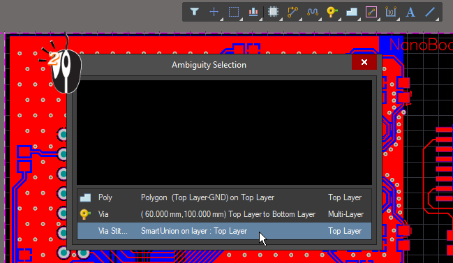
To select the array, switch the PCB panel to Unions mode and select the required Via Stitching or Via Shielding union. All vias that are part of that array will select, if the Select checkbox is enabled in the panel (as shown in the image below). Alternatively, double click on any via in the array to open the Add Stitching to Net dialog or the Add Shielding to Net dialog and edit the array.
 Use the PCB panel in Unions mode to select all vias in a stitching or shielding array. In this image all 4 via shielding unions are selected.
Selecting Interactively
Selection behavior:
- An individual stitching/shielding via can be selected and deleted.
- If the Popup Selection Dialog option is enabled (PCB Editor - General page of the Preferences dialog), clicking on an individual via that belongs to a union will display a list that includes the union, as shown in the image above. When a union is selected, it can be deleted.
- If the Popup Selection dialog is not enabled, then clicking on an individual via that belongs to a union will behave in the following way:
- The first click will select the individual via.
- The second and subsequent clicks will select the next object in the selection order used when there are overlapping objects: for example component, polygon, via union (if those objects are under the cursor).
- Alternatively, after the first click selects the individual via, press the Shift+Tab shortcut to invoke the Select Overlapping command. Continue pressing Shift+Tab to cycle through the overlapping objects, selecting each in turn.
- A stitching union that is constrained to an area can be selected by dragging a select-within window around any via in the union (drag left-to-right), as demonstrated in the animation in the Modifying a User-Defined Via Stitching Area section of this page.
Editing Stitching or Shielding Vias
The properties of a stitching or shielding via set can be edited once it has been selected, in the Via Stitching or the Via Shielding mode of the Properties panel.
 An example of an edit being performed to a via shielding.
As soon as any property has been edited in the panel, the Changes pending message and buttons appears at the bottom of the panel - use the appropriate button to complete your editing action.
Updating the Polygons After Editing a Stitching/Shielding Union
Once stitching is complete, you will need to re-pour the polygons if the applicable Polygon Connect Style design rule specifies a relief connection style. This can be done using the commands in the Tools » Polygon Pours sub-menu.
Further Reading
- For information about all aspects of PCB design, refer to the Printed Circuit Design and Fab Magazine website. The site is an excellent resource for technical topics, such as the role of a "via fence" (include the quote marks to improve the quality of the search results).
- Wikipedia article, Via Fence
- Studies on Via Coupling on Multilayer Printed Circuit Boards
- A paper that introduces the basic principals of EM wave propagation within a PCB structure - Best practice in circuit board design
- A discussion forum where the question Via fences for noise reduction of a chip antenna? was asked
- PCB design techniques for lowest-cost EMC compliance: part 1’ M K Armstrong. Electronics & Communications Engineering Journal Vol 11 No 4. IEE, August 1999.