The PCB is designed and formed as a stack of layers. In the early days of printed circuit board (PCB) manufacturing, the board was simply an insulating core layer, clad with a thin layer of copper on one or both sides. Connections are formed in the copper layer(s) as conductive traces by etching away (removing) unwanted copper.

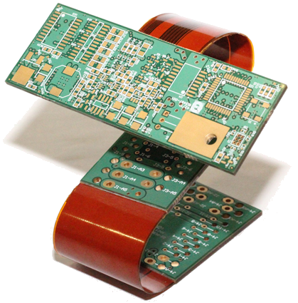
A single-sided PCB is shown on the left, typical of early PCB design. On the right is a rigid-flex PCB, where rigid sections are connected via flexible sections of PCB.
Fast forward to today, where almost all PCB designs have multiple copper layers. Technological innovation and refinements in the processing technology have led to a number of revolutionary concepts in PCB fabrication, including the ability to design and manufacture flexible PCBs. By joining rigid sections of PCB together via flexible sections, complex, hybrid PCBs can be designed that can be folded to fit into unusually shaped enclosures.
In printed circuit board design, the layer stack defines how the layers are arranged in the vertical direction, or Z plane. Since it is fabricated as a single entity, any type of board, including a rigid-flex board, must be designed as a single entity. To do this, the designer must be able to define multiple PCB layer stacks and assign different layer stacks to different zones of the rigid-flex design.
The Layer Stack Manager
The definition of the PCB layer stack is a critical element of successful printed circuit board design. No longer just a series of simple copper connections that transfer electrical energy, the routing of many modern PCBs is designed as a series of circuit elements, or transmission lines.
Achieving a successful, high-speed PCB design is a process of balancing the material selection and layer stackup and assignment, against the routing dimensions and clearances required to achieve suitable single-sided and differential routing impedances. There are also numerous other design considerations that come into play when designing a modern, high-speed PCB, including layer-pairing, careful via design, possible back drilling requirements, rigid/flex requirements, copper balancing, layer stack symmetry, and material compliance.
The Layer Stack Manager brings together all of these layer-specific design requirements into a single editor.
To open the Layer Stack Manager select Design » Layer Stack Manager from the main menus. The Layer Stack Manager opens in a document editor in the same way as a schematic sheet, the PCB, and other document types do.

All aspects of layer stack management are performed in the Layer Stack Manager.
As a standard document editor, the Layer Stack Manager (LSM) can be left open while the board is being worked on, allowing you to switch back and forth between the board and the LSM. All of the standard view behaviors, such as splitting the screen or opening on a separate monitor are supported. Note that a Save action must be performed in the Layer Stack Manager before changes are reflected in the PCB.
The functionality is divided over a number of tabs displayed across the bottom of the Layer Stack Manager:
Stackup Tab - add, remove and configure the layer properties of all layersExpand折叠
The Stackup tab details the fabrication layers. Layers are added, removed and configured in this tab. For a rigid-flex design, layers are also enabled and disabled in this tab.
- The properties of the currently selected layer can be edited directly in the grid, or in the Properties panel.
- Right-click in the layer grid, click the
 button, or use the Edit » Add Layer commands to add a layer. The new layer will be added next to the layer currently selected in the grid. Adding a Signal or Plane (copper) layer will also add a dielectric layer when an existing adjacent layer is also a copper layer.
- If the Stack Symmetry option is enabled in the Board section of the Properties panel, layers are added in matching pairs, centered around the mid-dielectric layer.
- The layer Material can either be typed into the selected Material cell or selected in the Select Material dialog, which is accessed by clicking the
 button.
- Surface Finish can be added to an outer copper layer by using the appropriate right-click sub-menu and adding a Surface Finish layer.
- Internal copper layers include a Copper Orientation option which defines the direction that the copper is bonded to the core (and then etched from). Configure this to ensure the impedance calculations are accurate.
- Copper layers also include an Orientation option. Configure this when a rigid-flex design has an internal/flex layer with components mounted on it, or when the design uses embedded components, to indicate the direction the component is oriented relative to that copper layer.
- The selected layer can be moved up or down within the layers of the same type using either the right-click or Edit menus.
- The Board section of the Properties panel includes options to enforce Stack Symmetry and Library Compliance, which are discussed below.
- The Substack section of the Properties panel displays a summary of the currently selected stack (or substack for a multi-stack rigid/flex design).
► Configuring the Stackup in the Properties panel
A maximum of 32 signal layers and 16 plane layers can be added.
Impedance Tab - configure the Impedance Profile requirementsExpand折叠
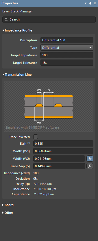
This tab is used to define impedance profiles, which can then be used with routing design rules.
- Click on the Impedance Tab at the bottom of the Layer Stack Manager to configure the Impedance Profile requirements. Once the impedance profiles have been configured, the required profile can then be selected in the Routing Width or
![]() Differential Pairs Routing design rules.
Differential Pairs Routing design rules.
- Click (or the Add Impedance Profile button if no profiles have been added yet) to add a new
![]() Impedance Profile, then define the required Type, Target Impedance and Target Tolerance in the Properties panel. The Description is optional.
Impedance Profile, then define the required Type, Target Impedance and Target Tolerance in the Properties panel. The Description is optional.
- The next step is to define which layers the currently selected profile is to be available on. The grid is divided into two zones: the layers in the stackup are displayed on the left, on the right are the layers that the currently selected impedance profile will be available on. Use the layer checkbox in the Impedance Profile region to enable that layer to be available for the selected impedance profile.
- When you select an enabled layer in the Impedance Profile region, all layers in the layer stack are faded, except those being used to calculate the impedance for that selected signal layer (show image
![]() ).
).
- Once the layer has an Impedance Profile assigned, edit that layer's reference layer(s) in the Top Ref and Bottom Ref columns. Note that reference layer(s) can be of Type Plane or Signal.
- The impedance calculators support forward and reverse impedance calculations. If you enter the Target Impedance, the Width will change automatically (forward calculation), or enter the Width and the Target Impedance will change automatically (reverse calculation).
- For a differential impedance calculation, lock either the Width or Trace Gap by clicking the appropriate
 button. The unlocked variable will then be calculated as the Target Impedance value is changed. Alternatively, edit the unlocked variable to change the Target Impedance.
- The Etch Factor
= Thickness/[(W1-W2)/2] (hover the cursor over the ? in the panel to display the formula)
- The impedance calculator supports multiple adjacent dielectric layers. These layers can have different dielectric properties.
- For a stripline structure, the dielectric height is calculated as the distance between copper layers (see H2 on the image
![]() ).
).
- The differential impedance calculator supports an asymmetric stripline structure.
- Single and differential coplanar structures are supported by the Simbeor impedance calculator.
- All calculations use a frequency of 1 GHz.
- To improve calculation speeds, impedance profiles are calculated in separate threads (when available).
Via Types Tab - define the allowed Z-plane layer-spanning requirements of the viasExpand折叠
The Via Types tab is used to define the allowed Z-plane layer-spanning requirements of the via(s) used in the design. The diameter and hole size (X&Y properties) of the vias placed in the design continue to be controlled by the default preferences if the via is placed manually, or the applicable Routing Style design rule if the via is placed during interactive routing.
- The Layer Stack for a new board includes a single, thruhole via span definition in the Via Types tab of the Layer Stack Manager. For a two-layer board, the default via is named Thru 1:2, the naming reflecting the via type, and the First and Last layers that the via spans. The default thruhole span cannot be deleted.
- Click the button to add an additional Via Type, then select the layers that this Via Type spans in the Properties panel. The new definition will have a name of <Type> <FirstLayer>:<LastLayer> (eg, Thru 1:2).
- The software will automatically detect the type (e.g., Thru, Blind, Buried) based on the layers chosen, and name the Via Type accordingly.
- If a µVia is required, enable the µVia checkbox. This option will be only available when the via spans adjacent layers, or adjacent +1 (referred to as a Skip via).
- If the Layer Stack has the Stack Symmetry option enabled, the Mirror option will become available. When Mirror is enabled a mirror of the current via, spanning the symmetrical layers in the layer stack, is automatically created.
- Vias placed in the workspace include a Name property dropdown, which lists all of the Via Types defined in the Layer Stack Manager. All vias used in the board must be one of the Via Types defined in the Layer Stack Manager.
- When you change layers during interactive routing:
- The Properties panel will display the applicable Via Type (show image
![]() ).
).
- If multiple Via Types are available to suit the layers being spanned, press the 6 shortcut to cycle through the available Via Types.
- The proposed Via Type is detailed on the Status bar (show image
![]() ).
).
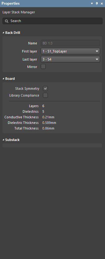
Back Drills Tab - define the layer-spans that are required to be back drilledExpand折叠
In a high-speed design, when the barrel of a via extends beyond the signal layers that the signal is routed on, signal reflections can occur. This can lead to signal degradation and signal integrity issues. One approach used to resolve this is to drill out the unused via barrels using controlled depth drilling, which is a technique also referred to as back drilling.
- Back drill properties are configured in the Back Drills tab, this tab appears when Back Drills are enabled in the Tools » Features sub-menu or by clicking the
 button then choosing Back Drills.
- The Back Drills tab is used to define the layer-spans that are required to be back drilled when there is a pad or via stub present. These settings are used in conjunction with the Max Via Stub Length design rule, where the maximum stub length and the drill oversize amount are specified. The Where the Object Matches setting in the rule can be used to restrict stub-removal to specific nets.
- Click the button to add a new back drill definition. The definition will be named according to the First layer and Last layer selected in the Back Drill section of the Properties panel, for example, BD 1:3. First layer defines the first layer to be drilled, Last layer defines the layer that drilling stops before (Last layer is the first layer in the layer stack that will not be back drilled).
- If the Substack Properties has the Stack Symmetry option enabled in the Properties panel, the Mirror option will become available in the Back Drill section of the panel. When this is enabled, a mirror of the current Back Drill is created, for example, BD 1:3 | 6:4.
Printed Electronics Stackup Tab - configure the layers for a printed designExpand折叠
Using modern printing technology, it is possible to print conductive and non-conductive layers directly onto a substrate material, building up an electronic circuit. This is referred to as printed electronics.
- The layer stack is configured for printed electronics by selecting the
![]() Tools » Features » Printed Electronics option. In this mode, all tabs are replaced by the single Printed Electronics Stackup tab.
Tools » Features » Printed Electronics option. In this mode, all tabs are replaced by the single Printed Electronics Stackup tab.
- Traditional dielectric layers are not used in printed electronics. Instead, local dielectric patches are printed where routing must cross over. When the Printed Electronics option is enabled in the Features drop-down, all dielectric layers are removed from the layer stack and instead, the dielectric patches are defined by placing suitably shaped region objects on non-conductive layers.
- In printed electronics, copper signal layers are referred to as conductive layers, and insulating layers are referred to as non-conductive layers.
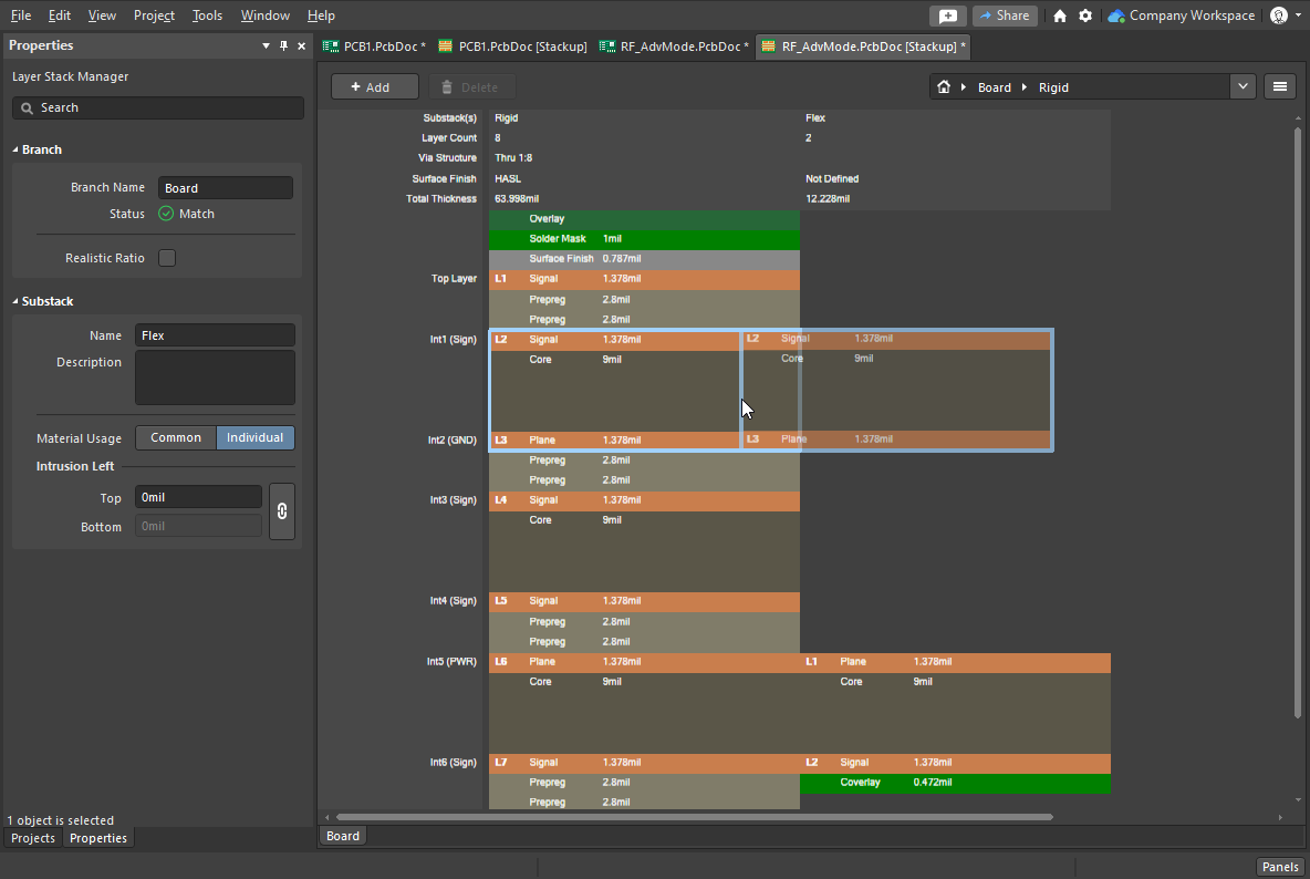
Board Tab - create and configure the substacks in a rigid-flex designExpand折叠
The Board tab is used to configure the different substacks required in a rigid-flex design. The Board tab is automatically displaying when Rigid-Flex (Advanced) mode is enabled. Note that it is not used/available when the standard Rigid-Flex mode is chosen.
The Board tab of the Layer Stack Manager is used to:
- Add Substacks. Additional substacks can be quickly created from an existing substack using the Shift+Click shortcut to select the required layers, and then dragging the selection horizontally to position it in the set of substacks.
- Configure the relationships between layers in adjacent Substacks - do they share layers (Common), or are the layers unique in that Substack (Individual).
- Configure if adjacent layers intrude into the neighboring Substack.
- Switch to editing a specific substack - double-click on it in the Board tab to do this.
- Add additional Branches. Branches are used when the design has multiple flex sections radiating from a single rigid section. Learn more about Branches.
The Board tab was introduced as part of the Advanced Rigid-Flex mode. Advanced Rigid-Flex supports design features such as overlapping flexible and rigid board regions, new Board Region and Bending Line behaviors, and the introduction of the Board tab in the Layer Stack Manager. You can switch between the standard Rigid-Flex mode and the Advanced Rigid-Flex mode by selecting the relevant command in the Layer Stack Manager, as shown below.
.") The interface changes as you select either the standard or Advanced Rigid-Flex mode (hover the cursor over the image to show the difference).
The interface changes as you select either the standard or Advanced Rigid-Flex mode (hover the cursor over the image to show the difference).
► Learn more about Designing a Rigid-Flex PCB.
Editing the Layer Stack Properties
The Layer Stack Manager presents the layer properties in a spreadsheet-like grid. The properties can be edited directly in the grid or they can be edited in the Properties panel. The panel can be used in each of the Layer Stack Manager tabs, for example, giving access to the impedance profile and transmission line properties in the Impedance tab, or the µVia settings in the Via Types tab.


Some of the different modes of the Properties panel in the Layer Stack Manager.
The Properties panel can be enabled/disabled via the  button at the bottom-right of the software.
When the Stackup tab of the Layer Stack document is active, the Properties panel allows you toedit the layer properties of the Layer Stack.

The Layer Stack Manager mode of the Properties panel: an overlay layer, an inner layer, a dielectric layer, and a plane layer.
- Name – the name of the layer.
- Manufacturer – the layer manufacturer.
- Material – the layer material. This can be pre-defined in the Altium Material Library dialog (Tools » Material Library) in the Constructions field, or user-defined in the Layer Stack. Click
 to open the Select Material dialog to choose the desired material for the currently selected layer in the layer stack.
- Thickness – the thickness of the signal layer.
- Dk – this is the Dielectric Constant (also referred to as εr in electromagnetics). This indicates the relative permittivity of an insulator material, which refers to its ability to store electrical energy in an electric field. For insulating purposes, a material with lower dielectric constant is better and in RF applications, a higher dielectric constant may be desirable. In addition, the lower the relative dielectric constant, the closer the performance of the material to that of air. This property is critical to matching the impedance requirements of certain transmission lines.
- Df – this is the Dissipation Factor. This indicates the efficiency of insulating material by showing the rate of energy loss for a certain mode of oscillation, such as mechanical, electrical, or electromechanical oscillation. In other words, this is the property of a material that describes how much of the energy transmitted is absorbed by the material. The greater the loss tangent, the larger the energy absorption into the material. This property directly impacts the signal attenuation at high speeds.
- Process – displays the copper plating process that is applied to the base copper that makes up the outer signal layers of the PCB (the Top Layer and Bottom Layer).
- Weight – the weight of the copper per unit area, usually expressed in ounces/square foot (e.g., 0.5 oz/ft2).
- Orientation – this defines which way the components point (orient) on that layer. For the top and bottom sides, this is set automatically in a new board. For other signal layers, it is used for:
- Rigid-flex designs, where components mount on an inner signal layer that becomes a surface layer on a flex section, the software needs to know which way those components point. Use the drop-down to select the required orientation. Choices include: Not allowed, Top, and Bottom.
- For a design that includes embedded components, the software needs to know which way a component points. Refer to the Designing a PCB with Embedded Components page for information regarding setting the component orientation in the layer stack. Use the drop-down to select the required orientation. Choices include: Not allowed, Top, and Bottom.
- Copper Orientation – this defines the direction that the copper is laminated onto the core. Use the drop-down to select Above or Below, which determines the direction from which it is etched.
The
Copper Orientation can also be chosen using the drop-down in the
Copper Orientation column of the
Layer Stack. To enable the column, right-click in the header, choose
Select columns then enable the
Copper Orientation entry in the
Select columns dialog. Also, the
Trace Inverted option in the
Impedance Profile mode of the panel can be used to configure the copper orientation.
The orientation can be configured using the Copper Orientation drop-down in the Stackup mode of the Properties panel in the Copper Orientation column (if it is currently displayed), or by the Trace Inverted checkbox in the Impedance Profile mode of the Properties panel.
- Pullback Distance – the distance from the plane edge to the board edge.
- Frequency – this is the frequency at which the material is tested and the value that Dk / Df correspond to a certain frequency. Frequency is also taken from material references.
- Description – enter a meaningful description.
- Constructions – for dielectric layers, this displays the constructions of the layer. The numerical reference relates to the structure of the woven glass fabric used in the dielectric layer material; these are standard references used by PCB fabricators.
- Resin – displays the resin percentage of the layer.
Notes on Constructions and Resin:
The choice of laminate construction can significantly impact both cost and performance. As should be expected, a single-ply construction will typically represent a cost savings compared to a multiple-ply construction. The magnitude of this savings will depend on the specific glass styles involved and a host of other parameters. Performance can also be affected and should be considered when specifying the constructions to be used. First, single-ply constructions are often lower in resin content. The other main benefit of single-ply constructions is dielectric thickness control, beyond resin content considerations. Tighter thickness tolerances can be achieved using a single-ply construction.
Constructions with relatively lower resin contents are often preferred since they result in less z-axis expansion and can therefore improve reliability in many applications. In addition, lower resin contents can also improve dimensional stability, resistance to warpage, and dielectric thickness control. On the other hand, constructions with higher resin contents result in lower dielectric constant values, which are sometimes preferred for electrical performance. In addition, a certain minimum resin content is required to ensure adequate resin-to-glass wet-out and to prevent voids from occurring within the laminate. The ability to wet out the glass filaments fully with resin is also important for CAP resistance.
- Material Frequency – this is the frequency at which the material is tested and the value that Dk / Df correspond to a certain frequency. Frequency is also taken from material references.
- GlassTransTemp – this is the Glass Transition Temperature (also known as TG) and is the temperature at which the resin changes from a glass-like state to an amorphous state changing its mechanical behavior, i.e. expansion rate.
- Note – enter any pertinent notes for the layer.
- Comment – enter any necessary comments for the layer.
- Stack Symmetry – enable to add layers in matching pairs, centered around the mid-dielectric layer. When enabled, the layer stack is immediately checked for symmetry around the central dielectric layer. If any pair of layers that are equidistant from the central dielectric reference layer are not identical, the Stack is not symmetric dialog opens.
When Stack Symmetry is enabled:
– An edit action applied to a layer property is automatically applied to the symmetrical partner layer.
– Adding layers will automatically add matching symmetrical partner layers.
- Library Compliance – when enabled, for each layer that has been selected from the Material Library, the current layer properties are checked against the values of that material definition in the library.
- Substack – this information is for the currently selected substack (layers, dielectric, thicknesses, etc.,). As you switch from one substack to another, this information will update accordingly (for the currently selected substack).
The Substack region will only be available if the Rigid/Flex option is enabled in the Features drop-down.
- Stack Name – enter the substack name. Naming the substack is useful when the X/Y stackup region is being assigned a layer substack.
- Is Flex – enable if the substack is flex.
- Layers – the number of conductive layers.
- Dielectrics – the number of dielectrics.
- Conductive Thickness – this is the sum of the thicknesses of all signal and plane layers (all copper or conductive layers).
- Dielectric Thickness – the thickness of dielectric layer(s).
- Total Thickness – the total thickness of the finished board.
- Roughness – shows roughness of conductive layers.
- Model Type – preferred model for calculating the impact of surface roughness (refer to the articles below for more information on the various models). Applies to all copper layers in the stack (should it be the substack?).
- Surface Roughness – value of the surface roughness (available from your fabricator). Enter a value between 0 to 10µm, default is 0.1µm
- Roughness Factor – characterizes the expected maximal increase in conductor losses due to the roughness effect. Enter a value between 1 to 100, default is 2.
To learn more about the options and controls available for the other Layer Stack tabs, use the links below:
Defining the Layer Stack
The layers you add in the Stackup tab of the Layer Stack Manager are the layers that will be fabricated during the manufacturing process.
 Layer properties can be entered directly into the grid, or selected from the Material Library.
The properties of a layer can be edited directly in the grid or in the Properties panel.
- Use the File » Load from File command to load an existing
*.stackup template (or the File » Load from Server command, if you use a Workspace).
- Use the File » Save As command to save the current stackup as a template (or the File » Save to Server command to save the template in your Workspace).
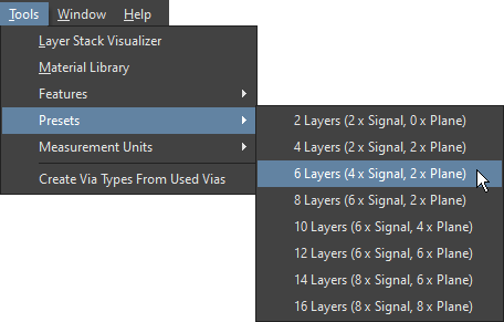
- Pre-defined layer stacks are also available, in the Tools » Presets menu.
Configuring the Layer Properties and Materials
The properties of each layer can be edited directly in the LSM grid, or a pre-defined material can be selected from the Material Library by clicking the ellipsis button () in the Material cell for the selected layer. The Stackup Tab collapsible section earlier on this page summarizes the various techniques available for adding, removing, editing, and ordering the layers.
User-defined property columns can be added and the visibility of all columns configured in the Select columns dialog. To open the dialog, right-click on any column heading in the grid region then choose Select columns from the context menu.
Layer Types and their Properties
There is a large variety of materials used in the fabrication of a printed circuit board. The table in the collapsible section below gives a brief summary of the common materials used.
Summary of layers types and their propertiesExpand折叠
The selection of layer materials and their properties should always be done in consultation with the board fabricator.
| Layer Type |
Materials Used |
Comments |
| Signal |
Copper |
Copper layer used to define signal routing carries the electrical signals and circuit supply current. Typically annealed foil and electro-deposited. |
| Internal Plane |
Copper |
Solid copper layer used to distribute power and ground; can be split into regions. Also must specify the distance from the plane edge to the board edge (pullback). Typically annealed foil. |
| Surface Finish |
Varies, including Electroless Nickel Immersion Gold (ENIG), Hot Air Solder Leveling (HASL), Lead-Free (HASL), Immersion Tin, Organic Solderability Preservative (OSP)/Entek, Hard Gold,
Immersion Silver
|
Applied to the exposed outer copper layers. Has two functions: to prevent oxidization of the copper, and provide a good surface for solder adhesion. Different pros and cons for each type of finish, the most popular is ENIG, offering high quality, good solderability and low cost. |
| Dielectric |
Varies, including FR4, polyimide, and a variety of manufacturer-specific materials offering different design parameters |
Insulating layer; can be rigid or flexible. Used to define core, prepreg and flexible layers.
Important mechanical properties are: including dimensional stability over moisture and temp ranges, tear resistance, and flexibility.
Important electrical properties include insulation resistance, dielectric constant (Dk), and dissipation factor (loss tangent, Df or Dj)
|
| Overlay |
Screen printed epoxy, LPI (liquid photo-imageable) |
Present text/artwork, such as component designators, logos, product name, and so on. |
|
Solder Mask/Coverlay
|
1) Solder Mask - Liquid photo-imageable solder mask (LPI or LPSM) , Dry Film photo-imageable Solder Mask (DFSM)
2) Coverlay - Adhesive coated flexible film, typically polyimide or polyester.
|
1) Protective layer that restricts where solder can be applied to the circuit. A cost-effective and proven technology, suitable for rigid and flex use class A (flex-to-install) applications. Suitable for finer features than flexible film coverlay.
2) Suitable for flex use classes A and B (dynamic flex). Requires rounded holes/corners, which are typically drilled or punched.
|
| Paste Mask |
Layer from which a paste mask stencil is fabricated. The stencil is typically stainless steel. Openings in the stencil define locations where solder paste is to be applied to the component pads prior to component placement. |
Mask layer used to fabricate the solder mask screen, which defines locations where solder paste is to be applied. |
Materials Library and Library Compliance
Dialog page: Altium Material Library
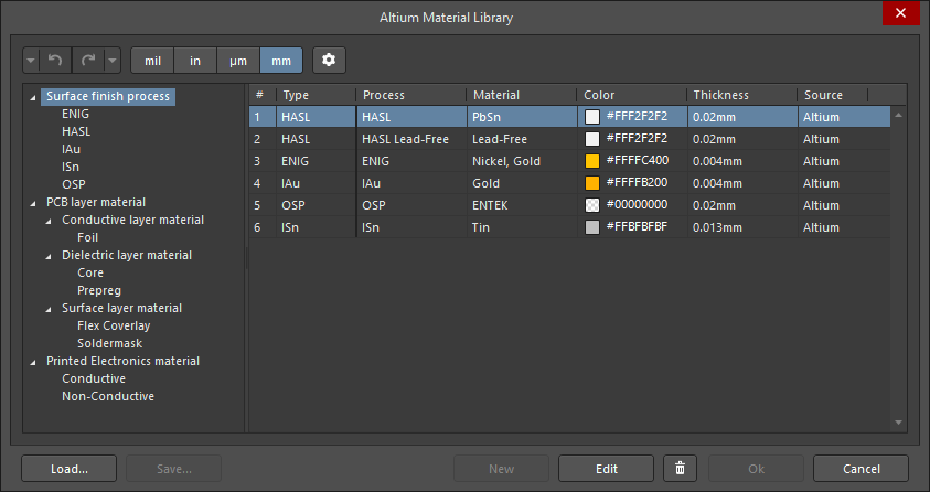
Preferred layer stack materials can be pre-defined in the Material Library. In the Layer Stack Manager, select Tools » Material Library to open the Altium Material Library dialog, where existing materials can be reviewed, and new material definitions added.
The material for a specific layer is not selected in the Altium Material Library dialog. To use a specific material for a layer, click the ellipsis () for that layer in the Materials cell of the layer stack grid. This will open the Select Material dialog, which restricts the library to only show materials suitable for the layer that the ellipsis control was clicked.
If the Library Compliance checkbox is enabled in the Layer Stack Manager, then for each layer that has been selected from the Material Library, the current layer properties are checked against the values of that material definition in the library. Any property that is not compliant is marked with an error flag. Re-select the material () to update the values to the Material Library settings.
Layer Stack Symmetry
Dialog page: Stack is not symmetric
If you require the board layer stack to be symmetrical, enable the Stack Symmetry checkbox in the Board region of the Properties panel. When this is done, the layer stack is immediately checked for symmetry around the central dielectric layer. If any pair of layers that are equidistant from the central dielectric reference layer are not identical, the Stack is not symmetric dialog opens.
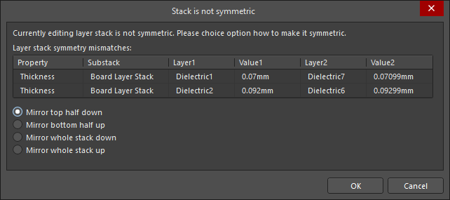
The upper section of the dialog details all detected conflicts in layer stack symmetry.
Options available to achieve layer stack symmetryExpand折叠
- Mirror top half down - the settings of each of the layers above the central dielectric layer are copied down to the symmetrical partner-layer.
- Mirror bottom half up - the settings of each of the layers below the central dielectric layer are copied up to the symmetrical partner-layer.
- Mirror whole stack down - an additional dielectric layer is inserted after the last copper (Surface Finish) layer, then all of the signal and dielectric layers are replicated and mirrored below this new dielectric layer.
- Mirror whole stack up - an additional dielectric layer is inserted before the first copper (Surface Finish) layer, then all of the signal and dielectric layers are replicated and mirrored above this new dielectric layer.
When Stack Symmetry is enabled:
- An edit action applied to a layer property is automatically applied to the symmetrical partner-layer.
- Adding layers will automatically add matching symmetrical partner-layers.
- Use the Stack Symmetry option as a quick way of defining a symmetric board - define half of the layer stack, enable the Stack Symmetry option, then use one of the mirror whole stack options to replicate that set of layers.
Layerstack Visualization
An excellent way to verify the layer stack is to visualize it in 3D.
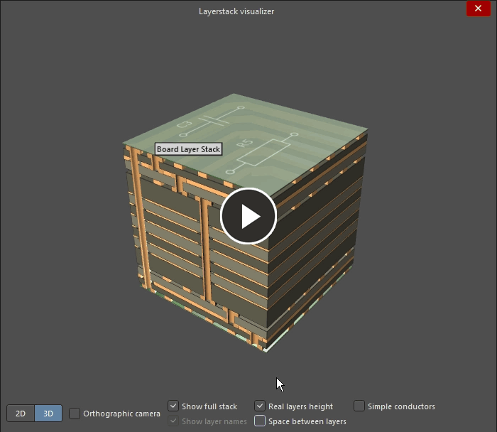
- Select Tools » Layerstack Visualizer in the Layer Stack Manager to open the Layerstack Visualizer.
- Use the controls to configure the presentation of the layer stack.
- Right-click and drag to reorient the board in the visualizer.
- Left-click on the image, then Ctrl+C to copy the image to the Windows clipboard.
Defining and Configuring the Rigid-Flex Substacks
Main article: Rigid-Flex Design
Rigid-Flex is under active development and now supports two modes of Rigid-Flex design. The original, or standard mode, referred to as Rigid-Flex, supports simple rigid-flex designs. If your design has more complex rigid-flex requirements, such as overlapping flex regions, then you need the Advanced Rigid-Flex mode (also known as Rigid-Flex 2.0). As well as overlapping flex regions, the Advanced mode also brings: visual definition of the substacks, easier definition of the rigid and flexible board regions, bends on nested cutouts, custom-shaped splits, and support for bookbinder-type structures. The required mode is selected in the Layer Stack Manager, as shown below.
The interface changes as you select either the standard or Advanced Rigid-Flex mode (hover the cursor over the image to show the difference).
► Learn more about Designing a Rigid-Flex PCB.
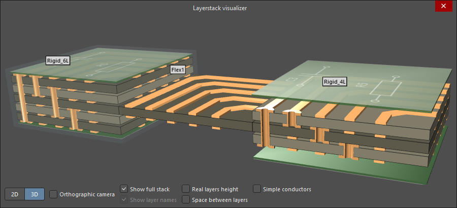
Each separate zone or region of a rigid-flex design can be made up of a different number of layers. To achieve that you need to be able to define multiple stacks, referred to as substacks.
Adding Substacks in a standard Rigid-Flex designExpand折叠
Adding Substacks in an Advanced Rigid-Flex designExpand折叠
- Enable the Rigid-Flex option by selecting the Tools » Features » Rigid/Flex (Advanced) command. You can also access the command in the Features ( ) menu.
- In Advanced Rigid-Flex mode the display will switch to show the Board tab, as shown below.
- There must be a unique substack defined for each unique set of layers needed in the rigid and flex regions of the overall board. Board mode is used to configure the different substacks required in an Advanced rigid-flex design.
- Additional substacks can be quickly created from an existing substack using the Shift+Click shortcut to select the required layers, and then dragging the selection horizontally to position it in the set of substacks, as shown in the image below.
- Configure the relationships between layers in adjacent Substacks - do they share layers (Common), or are the layers unique in that Substack (Individual).
- Configure if adjacent layers intrude into the neighboring Substack.
- Switch to editing a specific substack - double-click on it in the Board tab to do this.
- Add additional Branches. Branches are used when the design has multiple flex sections radiating from a single rigid section.
- For flex Substacks, enable the Is Flex option in the Properties panel. Flex-specific coverlay layers can only be added in a Substack that has the Is Flex option enabled and does not include a Soldermask layer.
► Learn more Designing a Rigid-Flex PCB
Other Layer-related Design Tasks
The layers in the layer stack form the space on which you build up the design. There are a number of design tasks that are related to the layers that are not performed in the Layer Stack Manager. These tasks are summarized below, with links to more information.
Defining the Board Shape
Main Article: Board Shape object, Board Region object, Bending Line object
Where the layer stack defines the board in the Z-plane, the Board Shape defines the board in the X and Y planes. Also referred to as the board outline, the board shape is a closed polygonal shape that defines the overall extent of the board. The Board Shape can be made up of a single Board Region (for a traditional rigid PCB), or multiple board regions (for a rigid-flex PCB).
The Board Shape can be:
- Defined manually - by redefining the existing shape, or placing one or more new board regions in Board Planning mode.
- Defined from selected objects - typically done from an outline on a mechanical layer. Use this option if an outline has been imported from another design tool.
- Defined from a 3D body - use this option if the blank board has been imported as a STEP model from an MCAD tool into a 3D Body Object (Place » 3D Body).
- Pulled directly from an MCAD package - Altium is developing direct ECAD - MCAD design technology, called Altium CoDesigner. Learn more about ECAD-MCAD CoDesign.
► Learn more about these approaches to defining the board shape.
► Once the shape has been defined, bends in the flexible sections of a rigid-flex design are defined by placing Bending Lines.
► Learn more about Rigid-Flex Design.
Assigning a Net to a Plane Layer
Panel page: Split Plane Editor
Related page: Internal Power & Split Planes
Assign a net to a plane layer, or a net to a split plane region, in the Split Plane Editor mode of the PCB panel.
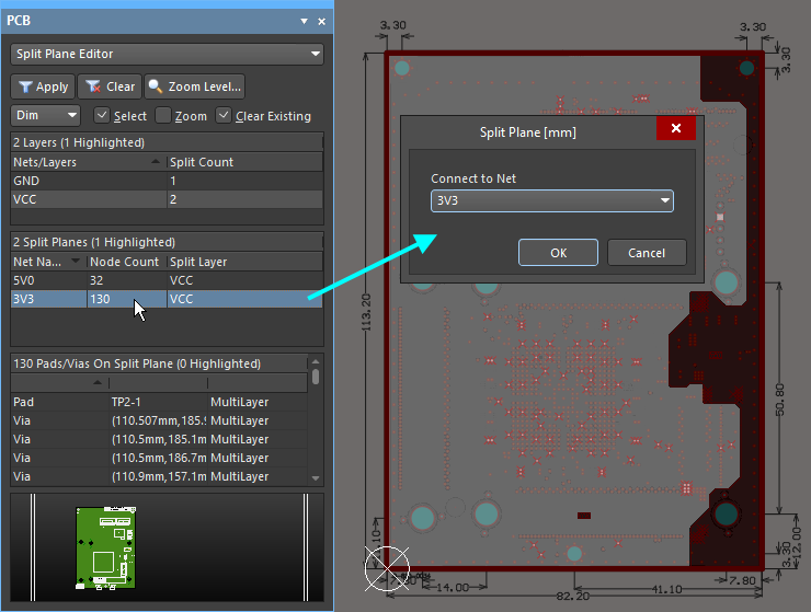
The panel lists all plane layers. When a layer is selected in the Layers section, the section below will list all of the split plane zones on that layer (there will only be one if the plane is continuous with no splits defined). Double-click on a split plane zone to open the Split Plane dialog, where you can assign a net. You can also double-click on the layer in the workspace (when the plane layer is the active layer) to open the dialog.
Configuring the Layer Stack for Components Mounted on an Internal Signal Layer
Related article: Embedded Components
There are two situations where components can be mounted on an internal signal layer:
- when there are embedded components, or
- when there are components mounted on a flex region of a rigid-flex board, and that flex layer extends from a mid-layer in the rigid section of the board.
The software needs to know which way components are oriented for each layer they are mounted on so that it knows when the component primitives must be mirrored. For the Top and Bottom Layers, this is configured automatically; for other layers, the setting is configured by the designer.
.") A component embedded on an internal signal layer (the component has been highlighted with blue outlines, the cavity with orange outlines).
A component embedded on an internal signal layer (the component has been highlighted with blue outlines, the cavity with orange outlines).
- Component orientation is configured for a layer in the Orientation column of the Stackup tab of the Layer Stack Manager.
- If the Orientation column is not visible, enable it by right-clicking on an existing heading in the layers grid then selecting Select columns from the context menu.
- The components on a layer can either point upwards (Top) or downwards (Bottom).
Documenting the Layer Stack
Object page: Layer Stack Table
Documentation is a key part of the design process and is particularly important for designs with a complex layer stack structure, such as a rigid-flex design. To support this, Altium NEXUS includes a Layer Stack Table, which is placed (Place » Layer Stack Table) and positioned alongside the board design in the workspace. The information in the layer stack table comes from the Layer Stack Manager.

Include a Layer Stack Table to document the design.
- To place a Layer Stack Table, select Place » Layer Stack Table.
- The Layer Stack Table details the:
- Layers used in the design
- Material used for each layer
- Thickness of each layer (and optionally the total board thickness).
- The Dielectric Constant
- The name of each stack and the layers used in that stack
- Double-click anywhere on the placed table to open the Properties panel in Layer Stack Table mode.
- The Layer Stack Table can also include an optional outline of the board showing how the various layer stacks are assigned to regions of the board. Use the Show Board Map option and slider bar to configure the map settings.
- The Layer Stack Table is an intelligent design object, meaning it can be placed and updated as the design progresses. Double-click on the Layer Stack Table to edit it in the Properties panel.
- An alternative approach to documenting the layer stack is to add a Draftsman document to the project and add a Layer Stack Table in it. Learn more about Draftsman.
Place the .Total_Thickness and the .Total_Thickness(<SubstackName>) special strings on a mechanical layer to include this information in your design documentation.
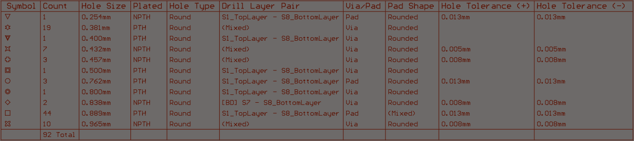
Including a Drill Table
Object page: Drill Table
Altium NEXUS includes an intelligent Drill Table that is placed like any other design object. The table can either display the drills required for all layer pairs (composite), or a specific layer pair. Place a drill table for each layer pair used in the design if you prefer separate drill information for each layer pair.
An alternative approach to documenting the layer stack is to add a Draftsman document to the project and add a Layer Stack Table in it. Learn more about Draftsman.
High Quality, Flexible Design Documentation
Main article: Draftsman
Altium NEXUS also provides a dedicated documentation editor - Draftsman. Draftsman has been built from the ground up as an environment for creating high-quality documentation that can include dimensions, notes, layers stack tables, and drill tables. Based on a dedicated file format and set of drawing tools, Draftsman provides an interactive approach to bringing together fabrication and assembly drawings with custom templates, annotations, dimensions, callouts, and notes.
Draftsman also supports more advanced drawing features including a Board Isometric View, a Board Detail View, and a Board Realistic View (3D view).
 Place drawing views, objects and automated annotations on single or multi-page Draftsman documents.
► Learn more about Draftsman
