Working with Object Specific Keepouts on a Board in Altium NEXUS
Parent page: PCB Placement & Editing Techniques
A Keepout in PCB design is a user-defined area or perimeter placed in the layout that copper objects cannot intersect. Typically included to control the area used by automated copper placement actions, such as polygon pours and interactive routing, a Keepout also represents an invalid location when manually placing copper objects.
As specified ‘no go’ areas during design layout, Keepout objects use the existing Clearance Constraint Rules to control routing and detect placement violations, but unlike other placed objects, cannot be assigned to a Net and are not shown in generated Outputs or printouts. In its simplest sense, a Keepout acts as an ‘interference’ object that prevents other copper objects from intersecting its area, as specified by the global Clearance Rule.
Altium NEXUS allows for the creation and application of Keepouts with its support for Object Specific Keepouts. Placed Keepout objects can be configured to specify which type objects they apply to, such as tracks, copper areas, vias, and pads, which significantly enhances the flexibility and effectiveness of Keepouts.
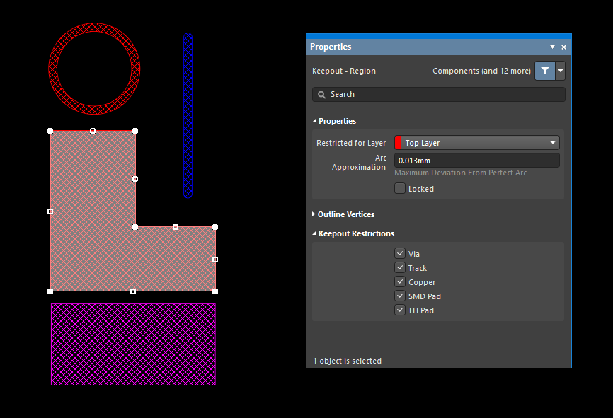
Keepout objects of different types placed in a PCB design.
In the PCB and PCB Library Editor, Keepout objects are displayed with cross-hatching. Keepout objects placed on the Keep-Out Layer (i.e. set to all signal layers) are shown in the Keep-Out Layer color, whereas Keepouts placed on a specific signal layer (i.e. set to this layer) appear in the color of this layer.
Keepouts are ideal for defining non-routable board regions (such as electrically sensitive or high voltage areas), specifically exposed copper locations such as in Fiducials and Test Points, or mechanically incompatible areas (such as mounting holes or the corners of a PCB). The configurable nature of Object Specific Keepouts also allows them to be placed over other objects when specific Keepout Restrictions have been assigned. When set to restrict only Vias, for example, a Keepout can be placed over existing copper regions (such as a Polygon Pour) to control the extent of automated Via Stitching.
Object Specific Keepouts can be placed in the PCB Editor and PCB Library Editor.
Placing Keepouts
A Keepout is placed in the editor design space from the Place » Keepout menu, where the nominated Keepout style (Track, Fill, Region, or Arc) will be placed on the currently active Layer. Select the Keepout’s Properties to edit its physical characteristics, layer or object type restrictions. The related Keepout properties are:
- Restricted for Layer – sets the Keepout Layer, and therefore the board layer on which copper objects will be restricted (kept out).
- Keepout Restrictions – determines which object types will be restricted by the Keepout. Deselecting an object type will cause the Keepout to allow transgressions by that type of object (not kept out), by not imposing the applicable Clearance Rule.
In the below image, the two Keepout Fills have different Layer and object restrictions applied. These allow the Top Layer Keepout Fill (on the left) to accept a Through Hole (TH) Pad while restricting all other object types, and the Keep-Out Layer (right) to accept tracks only.
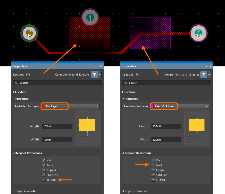
Example of two Keepout Fills placed on different layers of a PCB and configured to restrict placement of different object types.
The inherent flexibility of Keepouts allows their use for a wide range of tasks to control PCB layouts. Since Keepouts can be overlaid, assigned to any signal layer (such as Top or Bottom), and configured to reject specific objects, they can be used to tightly control Via Stitching and Polygon Pours, for example.
Polygon Pour Control
In the example PCB layout shown below, Keepout Fills have been added around the multilayer Pads in a region of potential high voltage, which needs to have sufficient electrical isolation from the pending ground-connected Polygon Pours. The Keepout Fills are set to Top Layer and configured to restrict only Copper objects, which will reject Polygon Pours, Fills and Regions while accepting existing tracks and pads, etc. – in other words, the Clearance violation Rule will only apply to objects classed as 'copper'.

Keepout Fills placed on the Keep-Out Layer and configured to be applied to copper objects only.
The above arrangement of Keepouts will force Polygon Pours placed on the signal layers (in this case the Top and Bottom Layers) to avoid all three Keepout areas. However, the top layer pads associated with the area of concern will not be provided with adequate clearance by the Top Layer Pour.
In this case, further Keepouts can be added to the Top Layer so that its Polygon Pour will avoid all the related pads by a suitable distance. In the image shown below, another two Keepout Fills have been added to the Top Layer, which is displayed here in Single Layer mode for clarity. Note that the Keepout coverage shown could have been created from a single Region, rather than two overlapping Fills.
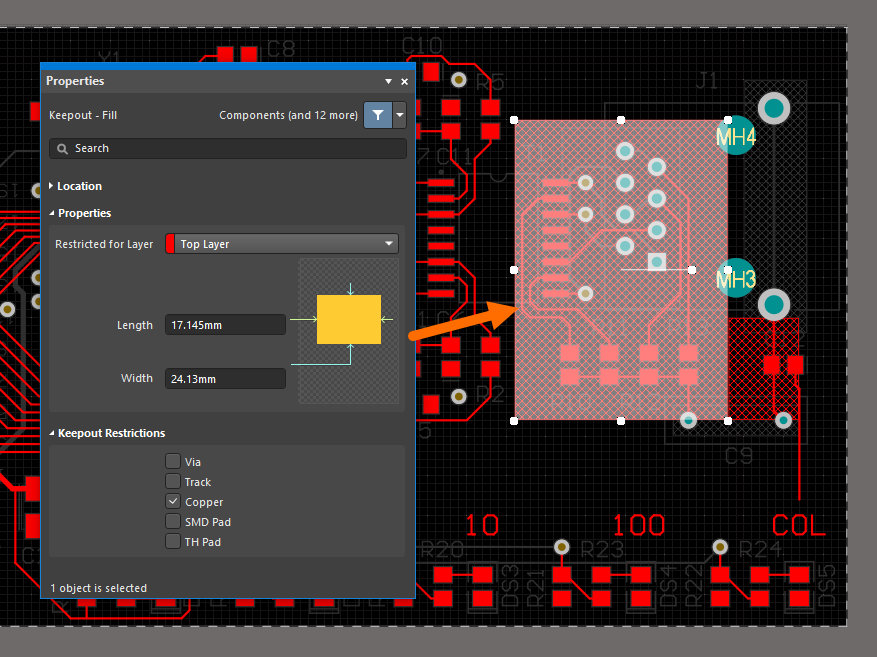
Keepout Fills placed on the Top Layer and configured to be applied to copper objects only.
When the Polygon Pours are eventually added to the layout, the collection of Keepouts will control the pours to produce a different clearance shape for each layer around the region. Note that in this example, the clearance associated with Keepouts is greater than that for normal objects due to a custom Keepout Clearance Rule (see below).
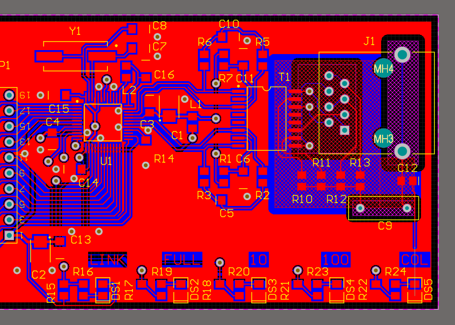
Polygon Pours avoid placed Keepout objects.
The influence of the Keepout collection on the Polygon Pours can be seen clearly when the layout is viewed in Single Layer 3D mode, as shown below – Top Layer on the left and Bottom Layer on the right.

The Top Layer (left) and Bottom Layer (right) of the PCB shown in Single Layer 3D mode.
Via Stitching Control
The application of Keepout shapes, configured to restrict Via objects, on multilayer copper areas can control the extent of automated Via Stitching (Tools » Via Stitching/Shielding). The Keepout shapes can be set for any layer or one of the copper area layers so that Vias between those layers will be ‘kept out’ (restricted).
In the example shown below, Keepout shapes have been added to the upper and lower left corners of the layout. These are configured to restrict Via objects, which will prevent the automated Via Stitching from placing Vias within those perimeters.
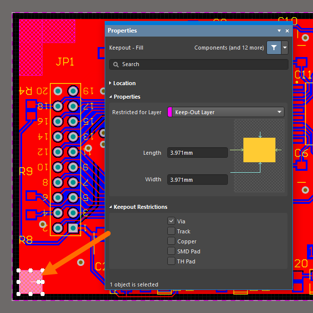
Keepout Regions configured to be applied to vias only.
Along with avoiding existing Tracks, Pads and Vias, as is normally the case, the Via Stitching also avoids the Keepout shapes as determined by the applicable Clearance Rule.
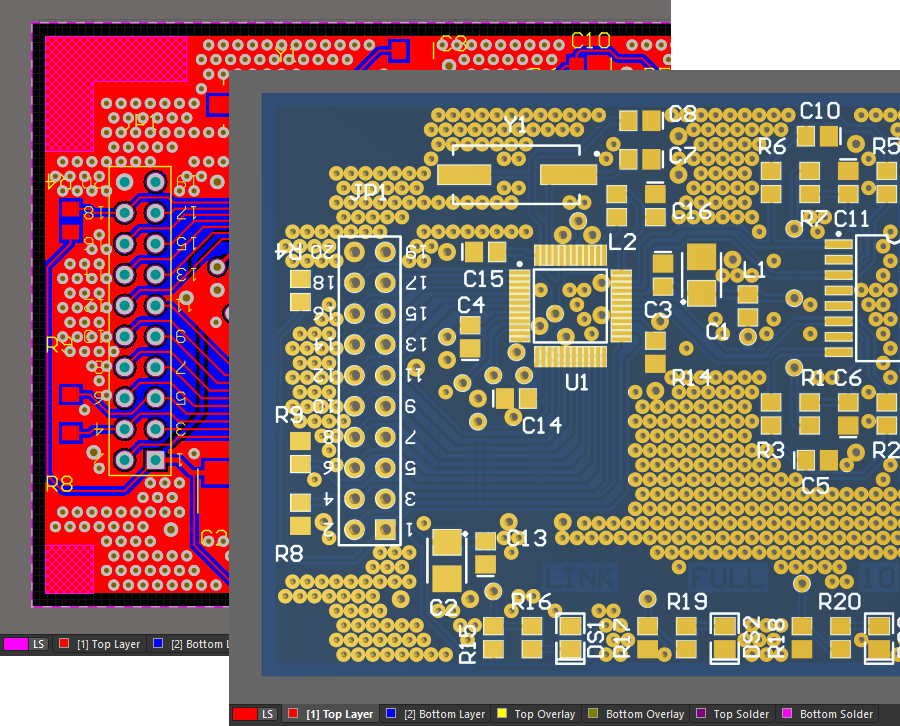
The PCB after adding via stitching.
Keepouts in Components
Keepouts are added to component Footprints in the PCB Library Editor using the same approach as those applied within the PCB Editor design space.
The Keepout added to the component Footprint shown below is configured to restrict all objects, but allow tracks – therefore enabling Net connections in a layout where the component is used, while restricting the close placement of other object types.
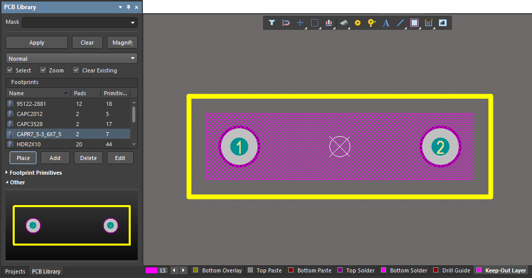
Keepout object can also be added to component footprints, in the PCB Library Editor.
Working with Keepouts
The implementation of Altium NEXUS’s Object Specific Keepouts is reflected in all associated functions, and includes compatibility with the Queries (and therefore Design Rules), the PCB List panel, and also imported/older PCB design documents.
Keepout Clearance Rule
As is the case for other object primitives, the current Electrical Clearance Rule will determine the clearance constraints for Keepouts – see Design » Rules. If a different clearance constraint is required for Keepouts, create a specific Rule by applying the IsKeepOut Attribute Check as a Custom Query.
Ensure that the custom Keepout Clearance Rule is set to a higher priority than the existing (global) Clearance Rule. In the example below, a rule has been created for Keepouts (Clearance_Keepout) with double the clearance constraint distance of the base Clearance Rule (Clearance). As shown in the section of board layout, the track routed between the two pads avoids the Keepout region (on the right) by a larger margin than the Top Layer region (left).
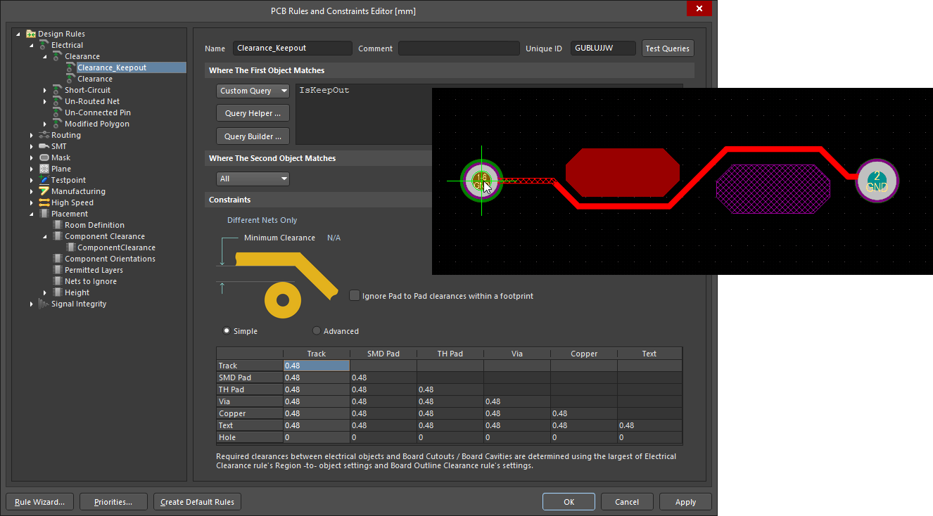
An additional Clearance rule for Keepout objects can be created.
Convert Primitive Objects to Keepouts
Existing primitive objects on signal layers can be converted to Keepouts, on the same layer, using the Convert Primitives to Keepouts command (Tools » Convert » Convert Selected Primitives to Keepout).

A primitive object can be converted to an equivalent Keepout object (and vice-versa).
Access via Panels
Object-specific Keepouts in a board design can be accessed via the PCB List and PCB Filter panels.
The PCB Filter panel allows the use of the IsKeepOut query keyword to locate and (optionally) select Keepouts objects in the design.
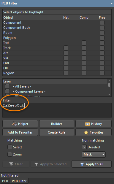
The PCB Filter panel can be used for locating Keepout objects in the design.
The PCB List panel can be used to list, select and edit the Keepout object of the selected type – for example, Keepout Fills, as shown in the below List panel image. A standard Top Layer Fill (the last listed) is also shown for comparison. If all the Fills (or other types of objects, such as Regions) included in the design are assigned as Keepouts, then the PCB List panel will include the full set of Keepout object Restriction attributes.

The PCB List panel can be used to list, select and edit the Keepout object of the selected type.
Importing PCB Designs
Altium NEXUS is able to import design files from a wide range of other design tools using the automated conversion capabilities provided by the Import Wizard (File » Import Wizard). Keepout type objects that are included in PCB design files from other design tools, some of which are object-specific, are converted to Object Specific Keepouts by the Wizard, where possible.
The Wizard’s Keepout conversion process is compatible with board designs from popular ECAD systems such as Mentor® Graphics Pads™ and Cadence® Allegro™. Correct Keepout interpretation also occurs during the IDF export process.
