
Working with a Component Object on a PCB in Altium NEXUS
 The component footprint defines the component mounting and connections on the PCB and can also include 3D
body objects to define the actual component.
Summary
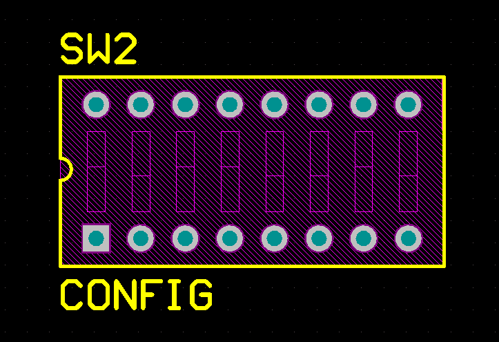
The component footprint defines the space and connection points needed to mount the physical component on the printed circuit board. It is a group object made up of a collection of simple primitive objects, which could include pads, lines and arcs, as well as other design objects. The pads provide the mounting and connection points for the component pins. Additional design primitives, such as lines and arcs, are often included to define the outline of the component shape on the component overlay (silkscreen) layer.
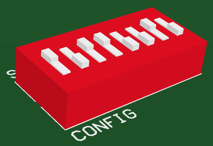
The component footprint can also include optional 3D body objects, which define the physical space or envelope of the actual component that is mounted on the board. If the physical component has been defined using 3D body objects or imported STEP models, three-dimensional component clearance checking can be performed.
Component footprints are created in the PCB Library Editor by placing suitable design objects to create the shape required to mount and connect the component. The component reference point is the origin of the Library Editor workspace, which can be set in the Library editor to: pin 1, the geometric center, or a user-defined location on the component.
To learn more about footprint creation, refer to Creating the PCB Footprint.
Availability
Component footprints are created in the PCB Library editor and placed in the PCB editor. To place a component in the PCB editor:
- Click Place » Component. If it is not active, the Components panel will open ready to locate the component required for placement.
- Select the component in the Components panel (View » Panels » Components), right-click then select Place <ComponentName>.
Placement
The process used to locate the required component footprint will depend on the method chosen to perform placement. Once the required footprint has been chosen for placement and is floating on the cursor:
- Press Tab to edit the properties of the component before it is placed.
- Press Spacebar to rotate the component counterclockwise (Shift+Spacebar for clockwise). The default rotation step is 90 degrees. To change this setting, use the Rotation Step value in the PCB Editor - General page of the Preferences dialog.
- If the component is being rotated, the Designator and Comment strings can be configured to hold their orientation, or to rotate with the footprint. This behavior is controlled by the Autoposition setting for these strings. The defaults can be set by editing the default Component on the PCB Editor - Defaults page of the Preferences dialog. Note that setting the default will not affect any components that have already been placed.
- Press the L shortcut to flip the component to the bottom side of the board. Do not use the X or Y keys as this will mirror the part but not change its layer.
Placing From the Components Panel
To place from the Components panel:
- To enable the desired libraries in the panel, click the
 then select then select File-based Libraries Preferences from the drop-down to open the Available File-based Libraries dialog. Use the dialog to add (on the Project tab) or select (on the Installed tab) a library.
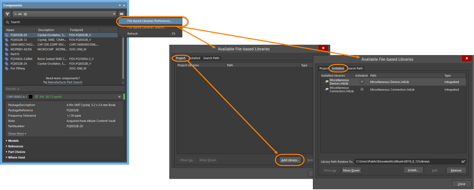
- Once footprint libraries have been enabled, the Components panel will refresh with the available components for that library.
With the part selected in the panel, placement of the component can be made in the following ways:
- Right-click then select Place <ComponentName> from the context menu.
- Double-click on the selected component. The component will appear floating in the workspace. Place the component in the desired location then click to place.
- Click and hold the component's name in the Components panel then drag the component to the desired location and click to place it. This is a 'single shot' placement technique, meaning only a single instance of the chosen component can be placed. The other methods allow multiple instances to be placed.
Graphical Editing
Graphical component editing is limited to moving, rotating and flipping. When a component is selected in the workspace it is highlighted in the current selection color as shown in the image below. To graphically manipulate a selected component:
- Press Delete to remove the selected component from the design.
- Click, hold and drag to move the selected component. The cursor will jump to the component reference point, or the nearest pad center if the Smart Component Snap option is enabled on the PCB Editor - General page of the Preferences dialog.
- While a component is moving on the cursor press the Spacebar to rotate it (Shift+Spacebar to rotate in the other direction).
- While a component is moving on the cursor press the L key to flip it to the other side of the board.
 Click once to select a component or click, hold and drag to move it.
Component Selection
When you click and select a component, the selection bounding box appears. Traditionally, the default bounding box behavior has been to use the smallest rectangle that encloses all of the primitives in that component, excluding the designator and comment strings.
To provide better support for more complex component shapes, the PCB.ComponentSelection Advanced Setting was added (click Advanced Settings on the System – General page of the Preferences dialog). This option gives the designer control over which layers are used to define the bounding box. After changing the PCB.ComponentSelection value in the Advanced Settings dialog, you will need to restart Altium NEXUS in order for the change to take effect.
The advanced option supports three modes (enter the value 0, 1 or 2, the default mode is 2):
- 0 - legacy mode - use all geometry from all layers, except the Designator and Comment strings.
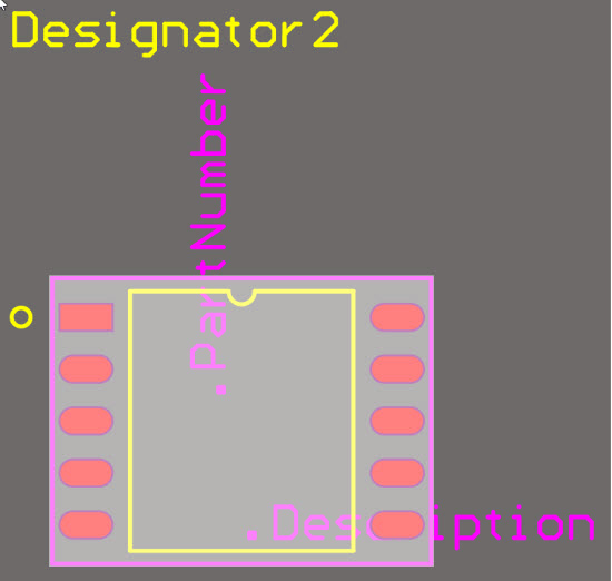
- 1 - by layer mode - use the geometries from the first of the layers listed below that contains objects, with the following priority:
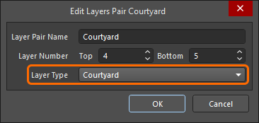
- Courtyard Layer (defined by the Layer Type property not the mechanical layer name, show image)
- 3D Body Layer (STEP models are stored in a 3D Body object sized to the smallest rectangular prism that holds the model. This 3D Body is used, not the shape of the STEP model)
- Silkscreen Layer plus Copper Layers
- Copper Layers
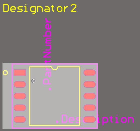
- 2 - by graphic mode - this mode uses geometries on the Courtyard layer; or when this layer is not present, combines geometries on the Silkscreen, 3D Body objects and Copper layers. Strings are excluded.
 show image
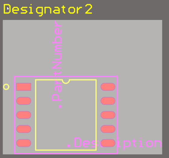
0 - legacy 1- by layer 2 - by graphic
Non-Graphical Editing
The following methods of non-graphical editing are available:
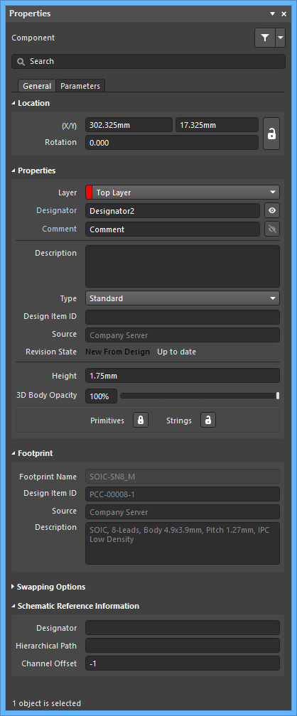
Editing via the Properties Panel
Properties page: Component Properties Panel
The properties of a Component can be edited in the PCB editor's Properties panel, which allows editing of all item(s) currently selected in the workspace.
During placement, the panel can be accessed by pressing the Tab key.
To access the properties of a placed component:
- Double-click on the component.
- Right-click on the component then select Properties from the context menu.
If the Properties panel is already active:
- Click once on the component to select it and access its properties in the panel.
Editing via the PCB List Panel
Panel page: PCB List, PCB Filter
The PCB List panel allows you to display design objects from one or more documents in tabular format, enabling quick inspection and modification of object attributes. Used in conjunction with appropriate filtering - by using the PCB Filter panel, or the Find Similar Objects dialog - it enables the display of just those objects falling under the scope of the active filter – allowing you to target and edit multiple design objects with greater accuracy and efficiency.