
Working with a Fill Object on a PCB in Altium NEXUS
Parent page: PCB Objects
 A placed Fill
Summary
A fill is a rectangular object that can be placed on any layer. When placed on a signal layer, a fill becomes an area of solid copper that can be used to provide shielding or to carry large currents. Fills of varying size can be combined to cover irregularly shaped areas and can also be combined with track or arc segments and be connected to a net.
Fills also can be placed on non-electrical layers. For example, place a fill on the Keep-Out layer to designate a 'no-go' area for auto-routing. Place a fill on a Power Plane, Solder Mask or Paste Mask layer to create a void on that layer. In the PCB Library Editor, fills can be used to define component footprints.
Availability
Fills are available for placement in both the PCB and PCB Library editors in the following ways:
- PCB Editor - the following methods of access are available:
- Choose Place » Fill from the main menus.
- Click the Fill button (
 ) in the drop-down on the Active Bar located at the top of the workspace. (Click and hold an Active Bar button to access other related commands. Once a command has been used, it will become the topmost item on that section of the Active Bar.)
 - Right-click in the workspace then click Place » Fill from the context menu.
- Click the button on the Wiring toolbar.
- PCB Library Editor - the following methods of access are available:
- Choose Place » Fill from the main menus.
- Click the Fill button () in the drop-down on the Active Bar located at the top of the workspace. (Click and hold an Active Bar button to access other related commands. Once a command has been used, it will become the topmost item on that section of the Active Bar.)
- Click the button on the PCB Lib Placement toolbar.
- Right-click in the workspace then select Place » Fill from the context menu.
Placement
After launching the command, the cursor will change to a cross-hair and you will enter fill placement mode. Placement is made by performing the following sequence of actions:
- Click or press Enter to anchor the first corner of the fill.
- Move the cursor to adjust the size of the fill then click or press Enter to anchor the diagonally-opposite corner and complete placement of the fill.
- Continue placing further fills or right-click or press Esc to exit placement mode.
Additional actions that can be performed during placement are:
- Press the Tab key to pause the placement and access the Fill mode of the Properties panel from where its properties can be changed on-the-fly. Click the workspace pause button overlay (
 ) to resume placement.
 - Press the L key to flip the fill to the other side of the board – note that this is only possible prior to anchoring the fill's first corner.
- Press the + and - keys (on the numeric keypad) to cycle forward and backward through all visible layers in the design to change placement layer quickly.
- Press the Alt key to constrain the direction of movement to the horizontal or vertical axis depending on the initial direction of movement.
Graphical Editing
This method of editing allows you to select a placed fill object directly in the workspace and change its size, shape or location graphically.
When a fill object is selected, the following editing handles are available:
 A selected Fill
- Click and drag A to resize the fill in the vertical and horizontal directions simultaneously.
- Click and drag B to resize the fill in the vertical and horizontal directions separately.
- Click and drag C to rotate the fill about its center point.
- Click anywhere on the fill away from editing handles and drag to reposition it. While dragging, the fill can be rotated or mirrored:
- Press the Spacebar to rotate the fill counterclockwise or Shift+Spacebar for clockwise rotation. Rotation is in accordance with the value for the Rotation Step defined on the PCB Editor – General page of the Preferences dialog.
- Press the X or Y keys to mirror the fill along the X-axis or Y-axis.
Non-Graphical Editing
The following methods of non-graphical editing are available:
Via the Properties Panel
Properties page: Fill Properties
This method of editing uses the associated Properties panel mode to modify the properties of a Fill object.
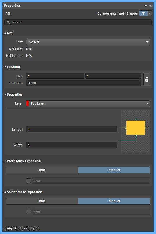
 The Fill mode of the Properties panel
During placement, the Fill mode of the Properties panel can be accessed by pressing the Tab key.
After placement, the Fill mode of the Properties panel can be accessed in one of the following ways:
- Double-click on the placed Fill object outline.
- Place the cursor over the Fill outline, right-click then choose Properties from the context menu.
- If the Properties panel is already active, select the Fill object.
Editing Multiple objects
The Properties panel supports multiple object editing, where the property settings that are identical in all currently selected objects may be modified. When multiples of the same object type are selected manually, via the Find Similar Objects dialog or through a Filter or List panel, a Properties panel field entry that is not shown as an asterisk (*) may be edited for all selected objects.
Via a List Panel
Panel page: PCB List, PCB Filter, PCBLIB List, PCBLIB Filter
A List panel allows you to display design objects from one or more documents in tabular format, enabling quick inspection and modification of object attributes. Used in conjunction with appropriate filtering - by using the applicable Filter panel, or the Find Similar Objects dialog - it enables the display of just those objects falling under the scope of the active filter – allowing you to target and edit multiple design objects with greater accuracy and efficiency.