
Working with a Fill Keepout Object on a PCB in Altium NEXUS

A Fill Keepout
Summary
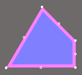
A fill is a primitive design object that can be placed on any layer. As well as the standard fill that is used for design tasks such as defining a component outline, there is a second type of fill available that is referred to as a fill keepout. A fill keepout can be placed as a layer-specific keepout object or an all-layer keepout to act, for example, as a placement or routing barrier. The difference between a standard fill and a keepout fill is that layer-specific keepout-type fills are not included in output generation, such as Gerber or ODB++. A keepout fill is identified by having an outline in the Keepout color.
Availability
Fill Keepouts are available for placement in both PCB and PCB Library Editors in the following ways:
- In the PCB Editor, place a keepout fill in the following ways:
- Click Place » Keepout » Fill from the main menus.
- Click the
 button in the graphic objects drop-down on the Active Bar menu located at the top of the workspace. (Click and hold an Active Bar button to access other related commands. Once a command has been used, it will become the top-most item on that section of the Active Bar.)
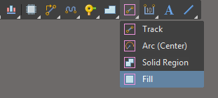
- Right-click then choose Place » Keepout » Fill from the context menu.
- In the PCB Library Editor, place a keepout fill in the following ways:
- Click Place » Keepout » Fill from the main menus.
- Click the button in the graphic objects drop-down on the Active Bar menu located at the top of the workspace. (Click and hold an Active Bar button to access other related commands. Once a command has been used, it will become the top-most item on that section of the Active Bar.)
Placement
After launching the command, the cursor will change to a cross-hair and you will enter fill keepout placement mode. Placement is made by performing the following sequence of actions:
- Click or press Enter to anchor the first corner of the fill keepout.
- Move the cursor to adjust the size of the fill keepout then click or press Enter to anchor the diagonally-opposite corner and complete placement of the fill keepout.
- Continue placing further fill keepouts or right-click or press Esc to exit placement mode.
Additional actions that can be performed during placement while the fill keepout is still floating on the cursor and before the first corner of the fill keepout is anchored are:
- Press the Tab key to pause the placement and access the Keepout - Fill mode of the Properties panel from where its properties can be changed on-the-fly. Click the workspace pause button overlay (
 ) to resume placement.
 - Press the Alt key to constrain the direction of movement to the horizontal or vertical axis depending on the initial direction of movement.

Graphical Editing
This method of editing allows you to select a placed object directly in the workspace and graphically change its size, shape or location.
When a fill keepout object is selected, the following editing handles are available:
- Click, hold and drag the corner handles to resize the fill keepout in the vertical and horizontal directions simultaneously.
- Click, hold and drag the side, top and bottom handles to resize the fill keepout in the vertical and horizontal directions separately.
- Click, hold and drag the middle handle to rotate the fill keepout about its center point.
- Click anywhere on the fill keepout away from editing handles then hold and drag to reposition it. While dragging, the fill keepout can be rotated or mirrored:
- Press the Spacebar to rotate the fill keepout counterclockwise or Shift+Spacebar for clockwise rotation. Rotation is in accordance with the value for the Rotation Step defined on the PCB Editor – General page of the Preferences dialog.
- Press the X or Y keys to mirror the fill keepout along the X-axis or Y-axis.
Non-Graphical Editing
The following methods of non-graphical editing are available:
Editing via the Properties Panel
Properties page: Fill Keepout Properties
The properties of a Fill Keepout can be edited in the PCB editor's Properties panel, which allows editing of all item(s) currently selected in the workspace.
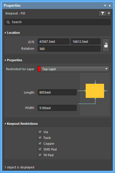 During placement, the panel can be accessed by pressing the Tab key.
To access the properties of a placed fill keepout:
- Double-click on the fill keepout.
- Right-click on the fill keepout then select Properties from the context menu.
- If the Properties panel is already active, select the fill keepout.
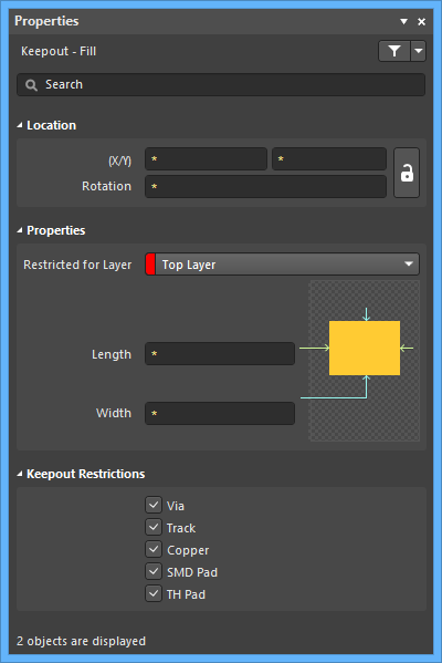
Editing Multiple objects
The Properties panel supports multiple object editing, where the property settings that are identical in all currently selected objects may be modified. When multiples of the same object type are selected manually, via the Find Similar Objects dialog or through a Filter or List panel, a Properties panel field entry that is not shown as an asterisk (*) can be edited for all selected objects.
Editing via the List Panel
Panel pages: PCB List, PCB Filter, PCBLIB List, PCBLIB Filter
The List panel allows you to display design objects from one or more documents in tabular format, enabling quick inspection and modification of object attributes. Used in conjunction with appropriate filtering by using the applicable Filter panel, or the Find Similar Objects dialog, it enables the display of just those objects falling under the scope of the active filter – allowing you to target and edit multiple design objects with greater accuracy and efficiency.