
PCB面板 - From-To编辑模式
Parent page: PCB Panel

The From-To Editor mode of the PCB panel
Summary
The PCB panel allows you to browse the current PCB design using a range of filter modes to determine which object types or design elements are listed, highlighted or selected. The panel also has editing modes for specific object types or design elements that provide dedicated controls for editing procedures. You also can access the properties for any element listed in the panel.
Use the From-To Editor mode of the PCB panel to add and remove user defined From-Tos. Predefined Topology options can also be selected using this panel to connect all nodes within selected nets.
Panel Access
When the PCB Editor is active, click the Panels button at the bottom-right corner of the workspace and select PCB from the context menu. Alternatively, you can access the panel through the View » Panels » PCB command.
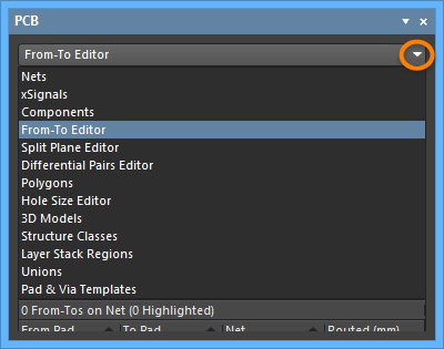
Once the PCB panel has been opened, select the From-To Editor option from the drop-down menu at the top of the PCB panel.
Setting the Visual Filtering
As you click on a net entry, all of the nodes on that net will be loaded into the middle region of the panel. Filtering will be applied and a mask automatically used in order to leave just the nodes (pads) on the net fully visible, with all other objects becoming dimmed.
 in the main editor workspace.")
Selecting a net lists its nodes in the PCB panel and displays them (as pads) in the main editor workspace.
Filter options
- Zoom checkbox - when enabled (default), the filtered objects will be zoomed and centered (where possible) in the design editor window. Use the Zoom Level button to adjust the zoom factor that will be used to close-in on filtered objects.
- Clear - use this button to disable the currently-applied filter. All objects in the design workspace will become fully visible and available for selection/editing. If you want to re-apply the filter, click the Apply button.
Using the From-To Editor
As you click on a net entry, all of the nodes on that net will be loaded into the middle region of the panel. Filtering will be applied and a mask automatically used in order to leave just the nodes (pads) on the net fully visible, with all other objects becoming dimmed.
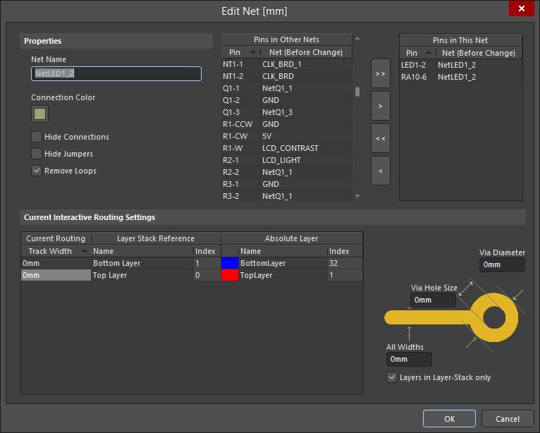
Double-clicking on a net entry will open the Edit Net dialog in which you can edit the properties of the net, including node membership.
Adding From-Tos
To add a user defined From-To between two nodes in a selected net, select the two nodes in the Nodes on Net region of the panel then click the Add From To button.
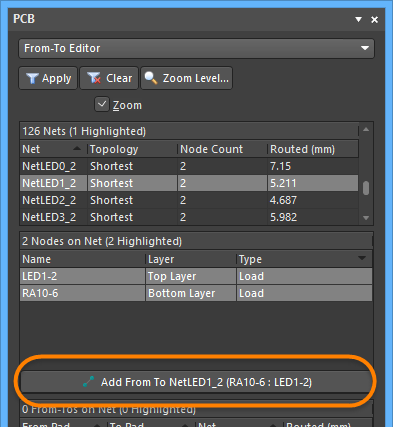
The newly added From-To will appear listed in the From-To on Net region of the panel and appears in the workspace as a dotted line between the two nodes.

A new From-To has been created on the net.
To remove a From-To, select its entry in the From-To on Net region of the panel then click the Remove button. Multiple From-Tos can be removed simultaneously. Use standard Ctrl+Click and Shift+Click features to multi-select entries in the list.
Choosing a Predefined Topology
The topology of a net is the arrangement or pattern of the pin-to-pin connections. By default, pin-to-pin connections of each net are arranged to give the shortest overall connection length.
A topology is applied to a net for a variety of reasons: for high speed designs where signal reflections must be minimized, the net is arranged with a daisy chain topology; for ground nets, a star topology could be applied to ensure that all tracks come back to a common point. You can either create dedicated From-Tos for node pairs in a net or you can choose to generate From-Tos for the net based on one of the predefined routing topologies available.
The following topologies are available and can be accessed from the From-To on Net region of the panel by clicking the Generate button:
- Shortest - this topology connects all nodes in the net to give the shortest overall connection length.
- Daisy Simple - this topology chains all the nodes together, one after the other. The order they are chained is calculated to give the shortest overall length. If a source and terminator pad are specified, then all other pads are chained between them to give the shortest possible length. If multiple sources (or terminators) are specified, they are chained together at each end.
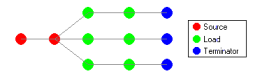
- Daisy Balanced - this topology divides all the loads into equal chains, the total number of chains equal to the number of terminators. These chains then connect to the source in a star pattern. Multiple source nodes are chained together.
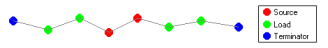
- Daisy Mid-Driven - this topology places the source node(s) in the center of the daisy chain, divides the loads equally and chains them off either side of the source(s). Two terminators are required, one for each end. Multiple source nodes are chained together in the center. If there are not exactly two terminators, the Daisy-Simple topology is used.
- Starburst - this topology connects each node directly to the source node. If terminators are present, they are connected after each load node. Multiple source nodes are chained together, as in the Daisy Balanced topology.
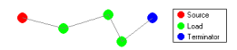
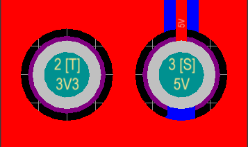
A pad can be defined as a Source, Terminator or Load by changing the entry for the Electrical Type field accordingly in the Pad mode of the Properties panel. Access to the Pad mode of the Properties panel is made by double-clicking on the entry for the pad in the Nodes on Net region.

Setting a pad's Electrical Type to Source in the Pad mode of the Properties panel.
When you change the electrical type for a pad to Source or Terminator, an "[S]" or "[T]" will be placed in the design workspace to distinguish it.
Panel Mini-viewer
The bottom section of the PCB panel provides a mini-viewer for the current document, with an image of the PCB board central to its window. A white viewing box is imposed on the image to show the area currently displayed in the design editor window. As the editor display automatically pans and zooms in response to the PCB panel filter selections, the box moves and expands accordingly to indicate the board viewing area.
As you manually pan around the document in the design editor window - using the editor's horizontal and vertical scroll bars or the right-click panning hand - the viewing box in the panel will also move accordingly. Conversely, if you click inside the viewing box and drag it around the board image, the document in the design editor window will be panned accordingly, and at the current zoom level.
As you zoom in or out in the design editor window, the viewing box will be resized accordingly in the panel. Conversely, resizing the viewing box in the panel, by clicking and dragging on any of its vertices, will cause the zoom level to change in the design editor window. The smaller the size of the viewing box, the more the actual document has been zoomed-in.