
KB: "Cannot Match Pads with New Footprint" Error During PCB Update
 Altium Designer
Solution Details
Footprint Update Blocked During ECO Processing
The error "Cannot match pads with new footprint in components: ..." appears during ECO processing and prevents the footprint from being updated in the PCB document.
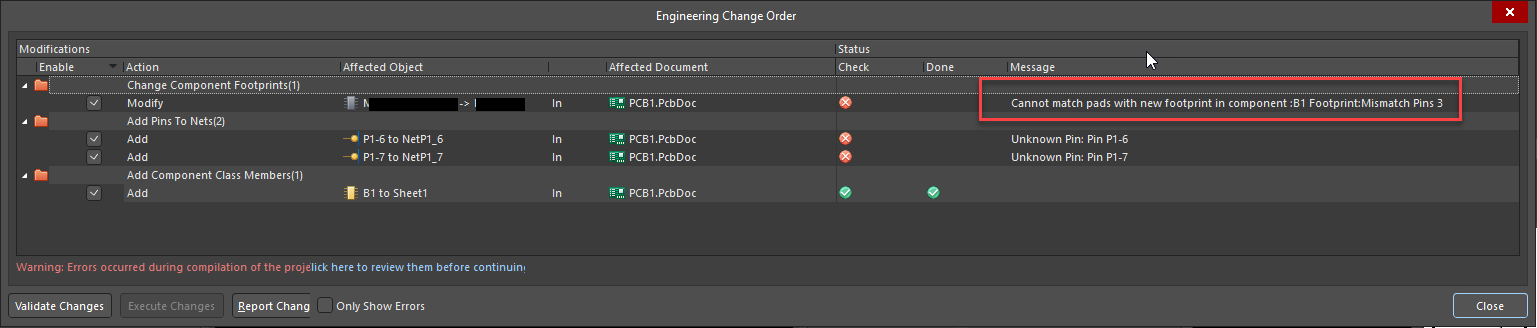
Pin and Pad Mapping Cannot Be Resolved
This issue occurs when the pin names, pin numbers, pad names, or pad numbers in the replacement footprint do not match those used in the existing footprint. Because netlist connectivity relies on these mappings, Altium Designer cannot safely remap the existing nets when the required pin-to-pad relationships are unavailable.
Verify Footprint Compatibility Before Updating
- Verify that the replacement footprint contains the same pin and pad numbers required by the existing connectivity.
- Update the footprint through the ECO process when the component or footprint revision has changed.
- Remove the existing footprint before importing the ECO if multiple pads have been consolidated into a single pad or the pad-numbering scheme has changed.
Verify Designators and Run the ECO Update Again
- Compare the pin names and pin numbers of the existing and replacement footprints.
- Compare the pad names and pad numbers of the existing and replacement footprints.
- Confirm that all pin-to-pad mappings required by existing net connections are present in the replacement footprint.
- If the replacement footprint changes the pad structure or numbering scheme, delete the existing footprint from the PCB document.
- Import the ECO again and apply the footprint update.
Example: Footprint Replacements That Generate the ECO Error
The following footprint is currently placed in the PCB document.
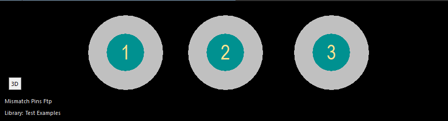
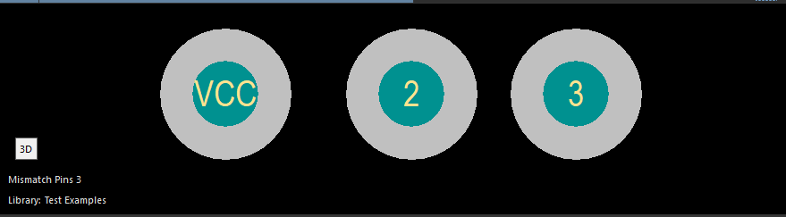
The replacement footprints shown below will both generate the ECO error because the required pin-to-pad mappings cannot be resolved.

Additional Notes
Component footprints can be changed freely. However, when netlist connections already exist, the replacement footprint must contain the pin numbers required by the previous footprint. If the required pin numbers are unavailable, the footprint substitution will be aborted.