
A Look at Creating File-based Library Components
This document outlines the creation of schematic components and PCB footprints, including adding 3D body objects, using the Schematic and PCB Library Editors in Altium Designer. A glossary of terms used in this document is included as an appendix.
The following topics are covered:
- Creating new libraries.
- Creating schematic components with single and multiple parts.
- Checking the components using Schematic Library Editor reports.
- Creating PCB component footprints manually and using the PCB Component Wizard.
- Handling other special footprint requirements, including irregular pad shapes.
- Including three-dimensional component detail (3D bodies).
- Checking the component footprints using PCB Library Editor reports.
- Creating an integrated library of the new components and models.
This information assumes you have working knowledge of the Schematic and PCB Editor environments and are familiar with placing and editing components.
Schematic Libraries, Models and Integrated Libraries
Schematic component symbols are created in schematic libraries (*.SchLib). The components in these libraries then reference footprints and other models defined in separate footprint libraries and model files. As a designer, you can place components from these discrete component libraries or you can compile the symbol libraries, footprint libraries and model files into integrated libraries (*.IntLib).
The advantages of Integrated libraries are that they are portable (everything is in one file) and the components and models in them cannot be edited. The bulk of Altium Designer components (around 70,000 ISO compliant components) are supplied in integrated libraries, which you will find in the Library folder of your Altium Designer installation. You can extract the source libraries out of an integrated library, to do this open the integrated library and choose Extract Sources to extract the source libraries, which will then be opened for editing. For more information, refer to Working with Integrated Libraries.
You can also create a schematic library of all the components that have been placed in the schematic documents of the active project by clicking Design » Make Schematic Library.
Creating Schematic Components
The Schematic Library Editor is used to create and modify schematic components, and manage component libraries. It is similar to the Schematic Editor and shares the same graphical design objects, with the addition of the Pin tool.
Components are created with the design objects in the Schematic Library Editor. Components can be copied and pasted from one schematic library to another or from the schematic editor to the schematic library editor.
Creating a New Library Package and Schematic Library
Before we start creating components, we need a new schematic library to store them in. This library could be created as a stand-alone library, referencing models in separate files. An alternate approach is to create the new schematic library with the intention of compiling it and the referenced models into an integrated library package. This means that before we create the library we need to create a new library package. A library package (*.LibPkg) is the basis of an integrated library - it binds together the separate schematic libraries, footprint libraries and model files that are ultimately compiled into the single integrated library file.

The new library, open at the default Component_1.
To create a new integrated library package and an empty schematic library, complete the following steps:
- Select File » New » Project to open the New Project dialog. In the Project Types region, select Integrated Library then click OK. A new library package named Integrated_Library1.LibPkg is created and displayed in the Projects panel.
- Right-click on the library package name in the Projects panel and select Save Project As. Browse to a suitable location, type in the desired filename then click Save. Note that the extension will be added automatically if you do not type it in.
- To add an empty schematic library select File » New » Library » Schematic Library. A new library named Schlib1.SchLib is created.
- Click File » Save As and save the library as Schematic Components.SchLib.
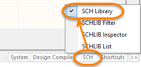
- If the Sch Library panel does not automatically open, click SCH » SCH Library near the bottom-right of the workspace.
Creating a New Schematic Component
To create a new schematic component in an existing library, you would normally select Tools » New Component. However, since a new library always contains one empty component sheet, we will simply rename Component_1 to get started on creating our first component, an NPN transistor.
- Select Component_1 from the Components list in the SCH Library panel and select Tools » Rename Component. Type the new component name that uniquely identifies it (for example, NPN) in the Rename Component dialog then click OK.
- If necessary, relocate the origin of the sheet to the center of the design window by selecting Edit » Jump » Origin (shortcut J, O). Check the Status line at the bottom left of the screen to confirm that you have the cursor at the origin. Components supplied by Altium are created around this point, marked with a cross-hair through the center of the sheet. You should always create your components close to this origin. When you place a component on the schematic, the component will be 'held' by the electrical hot spot (pin end) that is nearest this origin.
- The units, snap, and visible grids can be set in the Schematic Library Options dialog (Tools » Document Options, (shortcut T, D)). You can enable the Always Show Comment/Designator option in the Schematic Library Options dialog to display the Comment/Designator strings for the current component in your library document. Rather than opening the Schematic Library Options dialog whenever you need to change the grid, simply press G on the keyboard to quickly cycle through and set the Snap Grid to 1, 5, or 10 units.

Set the units and other sheet properties in the Schematic Library Options dialog.
Set the options in the Library Editor Options tab as shown in the above image. Open the Units tab and check the Use Imperial Units System option and ensure the Imperial unit used drop-down is set to Dxp Defaults.

The Units tab of the Schematic Library Options dialog.
Click OK to close the dialog. If the schematic library editor grid is not visible when the dialog is closed, press Page Up to zoom in until it is visible. Note that zooming occurs around the cursor, so keep the cursor close to the origin as you zoom in.
- To create the NPN transistor, we need to define the component body. Select Place » Line (shortcut P, L) or click the Place Line toolbar button (located in the Utilities toolbar drop-down).

The Place Line toolbar button
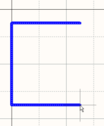
Using the following image and the grid lines as guides, place the vertical line. Click once to place the first end of the line then move the mouse to the location of the other end and click to place it, then right-click or press Esc to end placement of this line. Note that you are still in line placement mode, as indicated by the cross-hair on the cursor.

Placed NPN body
- For this transistor, the additional two lines are placed an an angle (the arrowhead will be placed in Step 6). Press Shift+Spacebar while you are placing a line to cycle through the different placement modes and find the angle mode which allows you to place the lines correctly. After defining the two angled lines, press Esc to exit placement mode.
- To create the arrowhead, select Place » Polygon (shortcut P, Y) or click on the Place Polygon toolbar button (located in the Utilities toolbar drop-down).

The Place Polygon toolbar button
Before placing the polygon, press the Tab key to open the Polygon dialog to define the properties. Set the Border Width to Smallest, enable Draw Solid, and set Fill Color and Border Color to the same color (example uses Basic 229) then click OK to close the dialog.

The Graphical tab settings of the Polygon dialog
In the workspace, click to place each vertex of the triangle (arrowhead) then right-click to end. Right-click or press Esc to end polygon placement mode. Double-click the placed polygon to open the Polygon dialog. Click on the Vertices tab in the dialog and set the vertices for the placed polygon. The image below shows the coordinates of the polygon vertices.

The Vertices tab settings of the Polygon dialog
- Save the component by clicking File » Save (shortcut Ctrl+S).
Adding Pins to the Schematic Component
Component pins give a component its electrical properties and define connection points on the component. They also have graphical properties. To place pins on the component:
- Select Place » Pin (shortcut P, P) or click on the Place Pin toolbar button (located in the Utilities toolbar drop-down).

The Place Pin toolbar button
The pin appears floating on the cursor, held by the electrical end that must be placed away from the component body, also referred to as the hot end. - Before placing the pin, press the Tab key to open the Pin Properties dialog to edit the pin's properties.

Define the pin attributes using the Pin Properties dialog.
- In the Pin Properties dialog, enter a pin name in the Display Name field (1 for the first NPN pin), and a unique pin number (also 1) in the Designator field. Enable the Visible options if you want the pin name and designator visible when you place the component on a schematic sheet.
- Set the Electrical Type of the pin from the drop-down list. This type is used when compiling a project or analyzing a schematic document to detect electrical connection errors in a schematic sheet. In this component example, all pins should have the Electrical Type set to Passive.
- In the Graphical region of the dialog, set the Length to 20 (all pins in this component will be set to 20) then click OK.
- Press the Spacebar to rotate the pin in 90º increments while it is floating on the cursor. Only one end of a pin is electrical (the hot end) and you must place the pin with this end out from the component body. The non-electrical end of the pin has the pin name next to it.
- Continue to add the pins required to finish the component, making sure the pin names, numbers, symbols, and electrical types are as shown in the following image.

NPN symbol with pin names and numbers visible.
- If you have placed all the pins with the Pin Name and Designator visible, you can easily change the display state of all in a single editing action. To do this select only the 3 pins (Shift+Click on each pin), press F11 to display the SCHLIB Inspector panel, and disable the Show Name and Show Designator options, as shown in the following image.

Editing the visibility of the pin name and number for all 3 pins.
- The drawing of your component is complete. Click File » Save to save it.
Notes on Adding Pins
- To set pin properties after placing the pin, double-click on the pin or double-click on the pin in the Pins list in the SCH Library panel to open the Pin Properties dialog. Alternatively, edit multiple pins in the SCHLIB Inspector panel as described above.
- Use "\" (backslash) after a letter to define an over-scored letter in a pin name.
- If you want to hide the power and ground pins on a component, enable the Hide option in the SCHLIB Inspector panel. When they are hidden, pins will be connected to power and ground nets as specified in the Connect To field, for example, the pin for VCC will connect to net VCC when placed.
- To view hidden pins or hidden pin names/numbers, click View » Show Hidden Pins from the main menus.
- You also can edit pin properties directly in the Component Pin Editor dialog without having to edit each pin through its corresponding Pin Properties dialog. Click Edit Pins in the Library Component Properties dialog (double-click on a component name in the SCH Library panel to open the dialog) to display the Component Pin Editor dialog as shown in the following image.

Review and edit all pins in the Component Pin Editor dialog.
- For a multi-part component, the relevant pins for the selected part will be highlighted with a white background in the Component Pin Editor dialog. All pins of other parts are grayed. You still can edit the pins of these non-selected parts. Select a pin and click Edit to display the Pin Properties dialog for that pin.
Setting the Schematic Component's Properties
Each component has properties associated with it such as the default designator, the PCB footprint and/or other models, and any parameters that have been defined for the component. Perform the following steps to set the component's properties:
- Select the component in the Components list of the SCH Library panel and click the Edit button or double-click on the component name to open the Library Component Properties dialog.
- Type in the Default Designator "Q?". Including the question mark allows the Designator to auto-increment upon placement (Q1, Q2, etc.,) if the designator is defined before placing the component (press Tab while placing to edit an object before placement).
- Enter a Comment that will display when the component is placed on a schematic sheet, e.g., NPN. Make sure the Visible options for the Default Designator and Default Comment fields are enabled. If the Comment field is left blank it will automatically be populated with the Symbol Reference when the component is placed.
- Enter a string into the Description field that describes the transistor, e.g., Transistor, NPN Generic. This string is searched during a library search and is displayed in the Libraries panel.
- Leave the other fields at their default values while we add models and parameters, as required.

Basic component properties are defined in the Library Component Properties dialog.
Adding Models to the Schematic Component
You can add any number of PCB footprint models to a schematic component, as well as model files that are used for circuit simulation and signal integrity analysis. If a component has multiple models (for example multiple footprints), you can select the appropriate model in the Library Component Properties dialog when you place the component on a schematic. In terms of sourcing the models, you can create your own or download a vendor's model file from the web. PCB libraries can include any number of PCB footprints.
Wherever possible, Spice models used for circuit simulation (.ckt and .mdl files) are included in the supplied integrated libraries in the Library folder of your Altium Designer installation. If you are creating a new component, you would typically source the Spice model from the device vendor's website. You can also use the XSpice Model Wizard (Tools » XSpice Model Wizard) to create certain Spice model types to add to the component.
The Schematic library editor's Model Manager dialog (Tools » Model Manager) enables you to view and organize your component models. For example, you can add the same model to multiple, selected components. Alternatively, you can add models to the current component by clicking on the Add button below the Model region in the SCH Library panel, or from the Model region of the workspace (click the upside-down arrow/caret symbol on the bottom right of the workspace as shown in the following image to access).

Click the highlighted caret symbol to access the Model region of the workspace.
Search Locations for Model Files
When you add a model to a component in the Schematic Library Editor, the model is linked; the model data is not copied and stored in the schematic component. This means the linked models must be available both during library creation and when the component is placed on a schematic sheet. When you are working in the library editor, the link from the component to the model information is resolved using the following valid search locations:
- Libraries that are included in the current library package project are searched first.
- PCB libraries (not integrated libraries) that are available in the currently Installed Libraries list are searched next. Note: The list of libraries can be ordered.
- Finally, any model libraries that are located down the Project search paths are searched. Search paths are defined in the Project Options - Search Paths Tab dialog (Project » Project Options). Note: Libraries that are down the search path cannot be browsed to locate a model, however, the compiler does include them when searching for a model.
Refer to the Understanding Models, Components and Libraries document for more information about the way models are searched for in the Schematic Library Editor and the Schematic Editor.
In this document, we will use different methods of linking the components and its model files. When the library package is compiled to create the integrated library, the various models are copied from their source locations into the final integrated library.
Adding Footprint Models to a Schematic Component
First, we will add the model that represents the component in the PCB Editor - the footprint (also known as a 'pattern' or 'decal' in other design tools). The footprint we will use for our schematic component is named "BCY-W3". When linking a PCB footprint model to a schematic component in the Schematic Library Editor, the model must exist in a PCB library, not an integrated library.
- In the Library Component Properties dialog, click Add in the Models region then select the desired Model Type from the drop-down in the Add New Model dialog (you also can click the drop-down arrow next to Add in the Models region to access the model types), and select Footprint from the list, as shown in Figure 13.

Adding a footprint model to the component.
- The PCB Model dialog (Figure 14) displays.

Use the PCB Model dialog to assign PCB models to schematic components.
- Click the Browse button to open the Browse Libraries dialog to browse footprint libraries that have been added into your library project.

Search for footprint libraries using the Browse Libraries dialog.
- If the desired footprint is not available in any of the current libraries, you will need to search for it using the Find button to open the Libraries Search dialog.
- Set the Scope to Libraries on Path and the Path to the appropriate folder. Ensure the Include Subdirectories option is enabled.
- In the query field at the top of the dialog, enter the appropriate Field and Value then click Search.

Searching the footprint libraries for the desired footprint in the Libraries Search dialog.
- Select the desired *.PcbLib file from the resulting Browse Libraries dialog then click OK to return to the PCB Model dialog.

Select the desired footprint in the Browse Libraries dialog.
- If this is the first time you have used this library, you will be asked to confirm the installation of this library, which will make it available for use. Click Yes in the Confirm dialog. The PCB Model dialog is updated with the footprint model information.
- Click OK to add the model. It will appear in the Model region at the bottom of the workspace.

The footprint model has been added to the component.
- After you added the model, it is a good idea to check the Pin-Pad mapping. To do this, open the PCB Model dialog (double-click the model in the Model region) then click Pin Map to open the Model Map dialog and make any necessary edits for the Pin-Pad pairs.

Make any necessary Pin-Pad mapping edits in the Model Map dialog.
Adding Component Parameters
Component parameters are a means of defining additional information about the component. This could include data your company needs in the BOM, manufacturer's data, a reference to the component datasheet, design instruction information, such as design rules or assignment to a PCB class, etc. Parameters can be used to add any useful information that you might need for a component and are configured in the Parameter Properties dialog.
Use the following steps to add a parameter to a schematic component:
- Double-click on the component name in the SCH Library panel to open the Library Component Properties dialog.
- Click Add in the Parameters region to open the Parameter Properties dialog.

- Enter the desired name of the parameter and a value. Ensure String is selected as the parameter Type in the Properties region if you require a text string and the value's Visible option is enabled if you want the value to display when the component is placed on a schematic sheet. Click OK . The parameter is added to the Parameters list in the Library Component Properties dialog.
Parameters for Component-to-datasheet Linking
Parameters can be used to create links from the component to reference material, such as data sheets. Linkage is established by adding specific component parameters. One approach is to use the F1 key to access a referenced document. The other, which caters to multiple references, uses the right-click context menu.
HelpURL
If a component includes a parameter with the reserved name HelpURL, then the URL will be resolved when the F1 key is pressed while the cursor is hovering over the component. The URL can actually be a web address, a text file, or a PDF file.
Component Links
The second technique supports multiple links and naming of each link. In this situation, you add a pair of parameters: one that points to the linked document or URL and the second that defines a label (or description) for the link. The parameter pairs are defined as follows.
|
|
Parameter Name |
Example Parameter Value |
|---|---|---|
|
1 st parameter |
ComponentLink1URL |
C:_ _My Datasheets\XYZDatasheet.pdf |
|
2 nd parameter |
ComponentLink1Description |
Datasheet for XYZ |
|
1 st parameter |
ComponentLink2URL |
C:_ _My Datasheets_ _Alternate XYZDatasheet.pdf |
|
2 nd parameter |
ComponentLink2Description |
Datasheet for Alternate XYZ |
Any number of links can be defined using the same parameter pair with the number incremented. When you right-click on a component that uses datasheet linking, a Reference menu entry appears with an entry for each component link in the sub-menu.

Right-click on a component in the workspace to access the datasheet links.
String Indirection
There might be instances when you need to define a placeholder that will be populated with text at a later time. For example, you might want a parameter called DesignedBy on a schematic template, whose value is defined when the template is used for a new schematic. Altium Designer uses a technique known as string indirection to support this requirement. At the schematic sheet level, you can add a document parameter whose value is left blank. You then place a standard string on the document, as n example "=DesignedBy". The equal sign sets this string to be an indirection string. Instead of displaying the text, it will display the current value of the document parameter DesignedBy.
String indirection can also be used with components. As well as displaying any parameter that has been added to the component in its own right by enabling the Visible option, you can also indirect the string to the component's Comment field.
One situation where string indirection is useful is for a component that is used for both PCB design and circuit simulation. During schematic-to-PCB design transfer, the schematic Comment field is mapped to the Comment field of the PCB component. However, for circuit simulation, the Comment field is not used since the simulator can require many properties for a component. For example, a BJT has five simulation properties and these five properties instead are defined as parameters. In this case, any of the circuit simulation parameters can be mapped to the Comment field using string indirection by entering the name of the parameter preceded by an equal sign ("="). For example, a resistor has one simulation parameter, called Value. If the resistor's Comment field is set to =Value , then the contents of the Value parameter will be displayed as the Comment. If you are tuning the resistance value during simulation, the correct resistance will be used when you transfer the design to PCB layout.
Checking the Component and Generating Reports
To check that the new components have been created correctly, there are three reports that can be generated. Ensure the library file is saved before the reports are generated.
Component Rule Checker
The Component Rule Checker tests for errors such as duplicates and missing pins.
- Select Reports » Component Rule Check (shortcut R, R) to open the Library Component Rule Check dialog.
- Set the attributes you want to check then click OK. A report titled <
libraryname.ERR> displays in the workspace that lists any components that violate the rule check.
- Make any adjustments necessary to the library and rerun the report.
- Save the schematic library. Close the report to return to the schematic editor workspace.
Component Report
The Component Report lists all the information available for the active component.
- Select Reports » Component (shortcut R, C).
- A report titled <libraryname.cmp> displays in the workspace and includes the number of parts with the pin details for each part in the component.
- Close the report to return to the schematic editor workspace.
Library Report
To create a extensive report of each component in the library:
- Select Reports » Library Report (shortcut R, L) to open the Library Report Settings dialog.

- Configure the report settings then click OK. The report will open in Microsoft Word or your web browser depending on the style chosen.
Copying Components from Other Libraries
You can also copy components to your schematic library from other open schematic libraries and then edit their properties as required. If the component is part of an integrated library, you will have to open the .IntLib file (File » Open) and choose Yes to extract the source libraries. Then open the generated source library (*.SchLib) from the Projects panel.
- Select the component that you want to copy in the Components list of the SCH Library panel so it displays in the design window.

Select a component to copy from the Components list in the SCH Library panel.
- Select Tools » Copy Component to open the Destination Library dialog that lists all currently open schematic library documents.
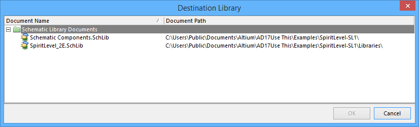
- Select the document to which you want to copy the component. Click OK and a copy of the component will be placed in the destination library where you can edit it, if necessary.
Copying Multiple Components
You also can use the SCH Library panel to copy multiple components. Select the components under Components in the panel using the standard Ctrl+Click or Shift+Click features, then right-click on one of the selected components and choose Copy from the pop-up menu. You can then right-click in the Components list and:
- Paste the component(s) back into the same library.
- Paste the component(s) into another open library.
- Copy and paste components from a schematic into an open library using the same technique.
Creating a New Schematic Component with Multiple Parts
The transistor symbol that you have created represents the entire component - this symbol represents what is supplied in the physical package delivered by the device manufacturer. There are situations where one physical component is better represented as a collection of parts. For example, there are resistor networks that contain eight individual resistors and each can be used independently of the others. Another example would be a 74F08 quad 2 input AND gate - in this device, there are four independent 2 input AND gates. While the component could be drawn as a single symbol showing all four gates, it would be more useful if it is drawn as four separate gates, where each gate can be placed independently of the others anywhere on the schematic. This approach of drawing a component as a set of separate parts is referred to as a multi-part component.
This section outlines the steps to create a 74F08SJX Quad 2-IN AND gate. We will also create an alternate view mode for the component, i.e., an IEEE representation of the device.
- In the Schematic Library Editor, click Tools » New Component (shortcut T, C) to open the New Component Name dialog.
- Type in the name of the new component, e.g., 74F08SJX, then click OK.

The new component name displays in the Components list in the SCH Library panel and an empty component sheet displays with a cross-hair through the center (origin) of the sheet.
- Now we will create the first part of the new component including its pins as described in the following sections. The first part will then be used as the basis for the other parts since only the pin numbers need to change between the parts.
Creating the Body of the Component
The body of this component is constructed from a multi-segment line and a circular arc. Make sure the component sheet origin is in the center of the workspace by selecting Edit » Jump » Origin (shortcut: J, O). Also, make sure the grid is visible (View » Grids).
Placing Lines
- Note the current grid setting displayed on the Altium Designer Status bar (bottom left). Set the grid to 5 by using the View » Grids command.
- Select Place » Line (shortcut P, L) or click on the
 Utilities toolbar. The cursor changes to a cross-hair and you are now in multi-segment line placement mode.
 - Press the Tab key to open the PolyLine dialog to set the line's properties. Set Line Width to Small .
- Refer to the X, Y co-ordinates at the left end of the Status bar, position the cursor at 25, -5, then click or press Enter to anchor the starting point of the line. Then position the mouse and click to anchor a series of vertex points that define the segments of the line (at 0,-5; 0,-35 and 25,-35).
- When you have finished drawing the line, right-click or press Esc to exit line placement mode.
- The completed polyline is shown below. Save the component.
Drawing an Arc
Placing an arc is a four-step process that sets the center point, radius, start angle, and end angle of the arc. You can press Enter instead of click to place the arc.
- Select Place » Arc (Center) (shortcut P, A). The last arc drawn appears on the cursor and you are now in arc placement mode.
- Press the Tab key to open the Arc dialog to set the arc's properties. Set the Radius to 15, Start Angle to 270, End Angle to 90, and the Line Width to Small. Use the Location region to define the coordinates: X: 25, Y: -20.
- There is no need to move the mouse since the cursor will jump to the correct location to define the Radius of 15 as set in the Arc dialog. Press Enter to accept the radius setting.
- The cursor will then jump to the start point of the arc, as set in the dialog. Without moving the mouse, press Enter to accept the arc start angle; when the cursor jumps again, press Enter again to define the arc end angle.
- Right-click or press Esc to exit Arc placement mode.
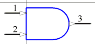
Adding Signal Pins
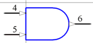
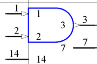
Add the pins using the same technique described in the Adding Pins to a Schematic Component section earlier in this tutorial. Configure Pins 1 and 2 with an Electrical Type of Input and Pin 3 is Output. Set the pin Length to 20. The completed part is shown below.
Creating Parts 2, 3, and 4
- Select the component by clicking Edit » Select » All (shortcut Ctrl+A) from the main menus.
- Click Edit » Copy (shortcut Ctrl+C) to copy to the clipboard.
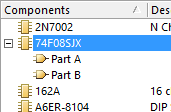
- Click Tools » New Part. A blank component sheet displays. In the SCH Library panel, the 74F08SJX component has been updated to include Part A and Part B. Click on the + to the right of the component name in the Components list in the SCH Library panel to view the new Parts.
- Click Edit » Paste (shortcut Ctrl+V). The outline of the component part will appear on the cursor. Place it at the same relative location to the sheet origin as Part A (the black cross-hair in the center of the sheet indicates the origin). If necessary, select and move the copied part until it is positioned the same as the original part.
- Update the pin information in the new part (Part B) by double-clicking on each pin and changing the pin name and number in the Pin Properties dialog. When complete, Part B will look like the image below.
- Repeat steps 3 through 5 above to create the remaining two parts, Parts C and D. Save the library.
Adding Power Pins
There are two approaches to defining the power pins:
- You can create a fifth part for the component and place the VCC and GND pins on that part. If you use this approach, remember to enable the Locked option in the Component Properties dialog to ensure that it cannot be swapped with any of the gates during re-annotation.
- The second approach is to define the power pins as hidden pins. In this case, the software automatically connects them to the specified nets.
Hidden power pins do not belong to any specific part in a multi-part component. They actually belong to all parts (ensuring they exist on the schematic regardless of which part has been placed). To support this requirement, pins can be assigned to Part 0 - a special part that is used to store pins that you want added to every part in the component. Perform the following steps to add hidden pins to the component:
- Add a pin to the component using the above instructions and set Display Name and Designator to 7; Electrical Type to Power; Enable Hide and enter GND in the Connect To text box; and set Part Number to 0. Display GND (pin number 7) pins to the component, setting their Part Number property to 0, Electrical Type to Power, Hide status to hidden, and Connect to net property to GND and VCC, respectively.
- Add another pin to the component using the above instructions and set Display Name and Designator to 14; Electrical Type to Power; Enable Hide and enter VCC in the Connect To text box; and set Part Number to 0.
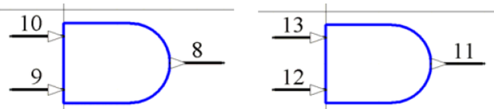
- To display the hidden objects, select View » Show Hidden Pins from the main menu. The completed part in shown in the image below. Check that the power pins appear on each part.
Setting the Component's Properties
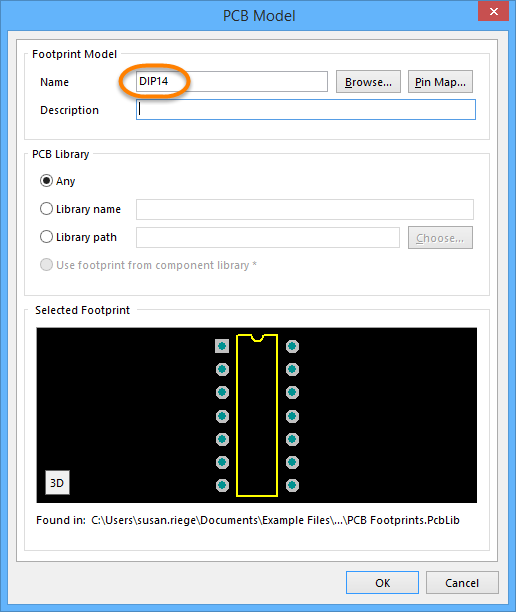
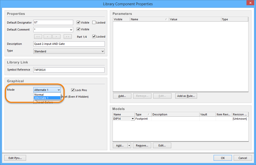
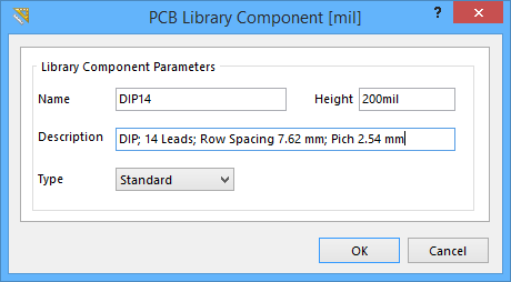
- Set the component's properties by clicking the Edit button in the SCH Library panel when the component is selected in the Components list. In the Library Component Properties dialog, set the Default Designator to U? and the Description to Quad 2-Input AND Gate. In the Models region of the Library Component Properties dialog, click Add then select Footprint in the Add New Model dialog then click OK. (You also can use the the drop-down of the Add button and select Footprint.) The PCB Model dialog opens. Enter DIP14 in the Name region as shown in the following image.
The Library Component Properties dialog now displays as shown in the following image. Click OK.

- Save the component in the library by selecting File » Save.
Creating an Alternate View Mode for a Part
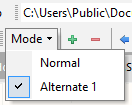
You can add many alternate view modes to a component part. These view modes can contain different graphical representations of the component, such as a DeMorgan or an IEEE representation. Each alternate view mode should always have the same set of pins as the Normal mode. If an alternate view of a part has been added, it is displayed for editing in the Schematic Library Editor by selecting the alternate mode from the Mode tool in the Mode toolbar.
To add an alternate view mode, with the component part displayed in the design window of the Schematic Library Editor:
- Select Tools » Mode » Add or click on the
 button in the toolbar region. A blank sheet for Alternate 1 displays.
 - Typically, you would copy the part you created in the Normal mode and paste it into the new Alternate mode. Use Edit » Copy and Edit » Paste to copy and paste the Normal mode to the Alternate mode. This gives you the correct set of pins and you can modify the graphical elements and position the pins as required.
- Click File » Save to save the library.
Once the component has been placed on a schematic sheet, the mode can be selected from the Mode drop-down list in the Graphical region of the Library Component Properties dialog as shown below.
IEEE Representations
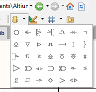
If a graphical IEEE representation needs to be added to the component, Altium Designer includes a selection of IEEE symbols. To access and place the symbols, use the IEEE toolbar (shown below) or click Place » IEEE Symbols.
Creating PCB Component Footprints
Footprints are always built on the top side, regardless of which final side of the board they are placed. Layer-specific attributes, such as surface mount pads and solder mask definitions, are automatically transferred to appropriate bottom-side layers when you flip the footprint to the other side of the board during component placement.
This section of the tutorial covers the following topics:
- Creating a new PCB library.
- Using the PCB Component Wizard to create a footprint for a schematic component.
- Manually creating a footprint.
- Other special footprint requirements, including irregular pad shapes.
- Including three-dimensional component body detail (3D bodies).
Footprints can be copied from the PCB Editor into a PCB library, copied between PCB libraries, or created from scratch using the PCB Component Wizard or drawing tools. If you had a PCB design with all the footprints already placed, you could use the Design » Make PCB Library command in the PCB Editor to generate a PCB library that includes only those footprints. Altium Designer also includes comprehensive libraries (*.PcbLib) of predefined through-hole and SMD component footprints for use in designing PCBs.
The footprints that are created manually in this part of the tutorial are only to illustrate the procedures required; they are not dimensionally accurate. Always check the specifications of a new footprint against the manufacturer's datasheet.
Creating a New PCB Library
To create a new PCB library:
- Select File » New » Library » PCB Library. A new PCB library document named PcbLib1.PcbLib is created and an empty component sheet called
PCBComponent_1displays. - Rename the new PCB library document to PCB Footprints.PcbLib, for example, by selecting File » Save As. The new library PCB Footprints.PcbLib displays in the Projects panel.
- Open the PCB Library panel.
- Click once in the grey area of the PCB Library Editor workspace and press Page Up or Page Down as needed until you can see the grid.
You are now ready to add, remove, or edit the footprint components in the new PCB library using the PCB Library Editor commands.
Using the PCB Component Wizard
The PCB Library Editor includes a PCB Component Wizard that will build a component footprint using information you supply. We will use the Wizard to create a footprint for a DIP14.
Perform the following steps to create the new component footprint DIP14 using the Component Wizard:
- Select the Tools » Component Wizard. The PCB Component Wizard will open. Click Next to progress through the pages of the Wizard.

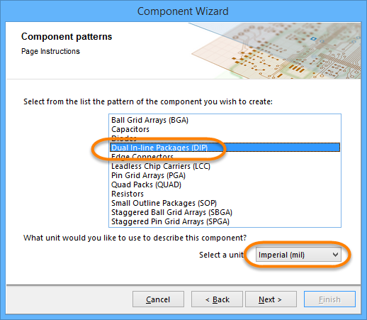
- Select Dual in-line Packages (DIP) and Imperial (mil) on the Component patterns page.
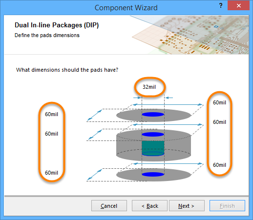
- Select each dimension and type in the new dimensions as follows: 60mil for the round pads and 32mil for the hole dimension.
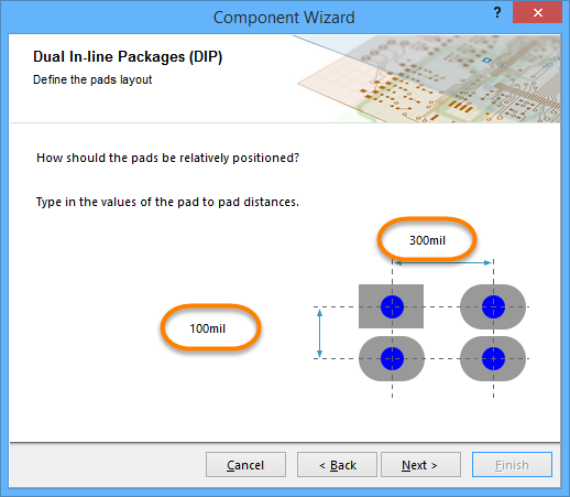
- Select and type the new pad to pad distances: 300mil (horizontal) and 100mil (vertical).
- Leave the outline width page at the default setting. Set the number of pads to 14 on the following page.
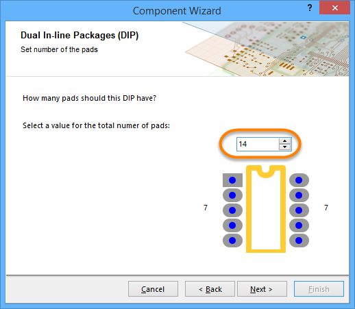
- On the next page, ensure the name is displayed as DIP14. Click Finish on the last page of the Wizard. The filename of new footprint (DIP14) will appear in the Components list in the PCB Library panel and the new footprint will display in the design window, as shown in the following images.

DIP14 has been added to the PCB Library panel.

DIP14 component that was created using the PCB Component Wizard.
- Click File » Save to save the library with its new footprint component.
Using the IPC® Compliant Footprint Wizard
You also can create component footprints using the IPC Compliant Footprint Wizard. Rather than requiring you to enter the properties of the pads and tracks that are used to define the footprint, the IPC® Compliant Footprint Wizard takes the actual component dimensions as its inputs. Based on the formulae developed for the IPC-7351 standard, the Wizard generates the footprint using standard Altium Designer objects, such as pads and tracks. The Wizard is launched from the PCB Library Editor by clicking Tools » IPC Compliant Footprint Wizard. Click Next to progress through the pages of the Wizard, setting the options as desired on each page.

The IPC Compliant Footprint Wizard builds the footprint based on the component dimensions.
Manually Creating a Footprint
Footprints are created and modified in the PCB Library Editor using the same set of tools and design objects available in the PCB Editor. Anything can be saved as a PCB footprint, including corner markers, phototool targets, and mechanical definitions. Once a footprint has been placed onto a PCB, you can set the Type property, defining it as Graphical or Mechanical if required.
To create the component footprint, we will place pads to form the component pin connections then place tracks and arcs for the outline. Design objects can be placed on any layer, however the outline is normally created on the Top Overlay (silkscreen) layer and the pads on the multi-layer (for thru hole component pins) or the top signal layer (for a surface mount component pins). When you place the footprint on a PCB, all objects that make up the footprint will be assigned to their defined layers.
To manually create a footprint suitable for the NPN transistor:
- Before creating the footprint, check that the units and grids are suitable. Select Tools » Library Options (shortcut D, O) to display the Board Options dialog. Ensure that Unit is set to Imperial and enable Snap To Grids in the Snap Options region. Open the Grid Manager dialog by clicking Tools » Grid Manager from the main menus, then double-click on a listed item to open the Cartesian Grid Editor dialog. In the Steps region, set Step X and Step Y to 10mil using the associated drop-downs.
- To create an empty component footprint workspace, click Tools » New Blank Component (shortcut T, W) from the main menus.
- To rename the default blank footprint, double-click on its name in the PCB Library panel to open the PCB Library Component dialog. Enter the same name as the one used earlier in the tutorial (BCY-W3).
Placing Pads on a New Footprint
The Pad properties dialog has a viewer that allows you to inspect the pad shapes on the defined layers. You can define normal circular, oval (slotted), or square holes in pads and toggle their plated property (plated or unplated) and all the work needed to support thermal reliefs generation, clearances calculation, output to Gerber, ODB++, and NC Drill, for example, will be automatically handled. The NC Drill Output (NC Drill Excellon format 2) will generate up to six different NC files for three different hole kinds and whether or not they are plated or non-plated.
To place the pads:
- Select Place » Pad (shortcut P, P) or click
 on the toolbar. A pad will appear floating on the cursor. Before placing the first pad, press the Tab key to open the Pad dialog to define the pad properties.
 - Edit the various regions of the dialog as shown in the following image. This creates a stretched round pad.
- Using the coordinates displayed in the Status bar, position the first pad at X:0, Y:-50, and click or press Enter to place.
- After placing the first pad, another will appear on the cursor. Position the cursor at X:0, Y:0 then click to place the second pad. The pad designator is automatically incremented.
- Position the cursor at X:0, Y:50, then click to place the third pad.
- Right-click or press Esc to exit pad placement mode. The three pads should resemble the following image.
- Save the footprint by selecting File » Save (shortcut Ctrl+S).
Pad Designators
Pads can be labeled with a designator (usually representing the component pin number) of up to 20 alphanumeric characters. The designator can be left blank if desired. If the designator begins or ends with a number, the number will auto-increment when placing a series of pads sequentially. To achieve alpha increments, e.g,. 1A, 1B, or numeric increments other than 1, use the Setup Paste Array dialog (click the Paste Array button in the Paste Special dialog (Edit » Paste Special)).
Paste Array Feature
By setting the designator of the pad prior to copying it to the clipboard, you can use the Setup Paste Array dialog to automatically apply a designation sequence during pad placement. By using the Text Increment field in the Setup Paste Array dialog, the following pad designator sequences can be placed:
- Numeric (1, 3, 5)
- Alphabetic (A, B, C)
- Combination of alpha-numeric (A1 A2, or 1A 1B, or A1 B1 or 1A 2A, etc.)
To increment numerically, set Text Increment field to the amount you wish to increment by. To increment alphabetically, set the Text Increment field to the letter in the alphabet that represents the number of letters you wish to skip. For example, if the initial pad has a designator of 1A, set the field to A, (first letter of the alphabet), to increment designators by 1. If you set the field to C (third letter of the alphabet), the designators will become 1A, 1D (three letters after A), 1G, etc.
Drawing the Outline on the Component Overlay
The outline that appears on the PCB silkscreen is defined on the Top Overlay layer. If the component is flipped to the bottom of the board during placement, the overlay is automatically transferred to the Bottom Overlay layer.
- Click on the Top Overlay layer tab at the bottom of the main editing window before placing overlay objects such as arcs or lines (tracks).
- To place the arc, select Place » Arc (Center) from the main menus. Position the cursor at X:0, Y:0 then click to define the arc center then edit the placed arc through the settings in the Arc dialog.
- Click to approximately define the arc radius, then click to define the arc start angle. Click again to define the arc end angle. Right-click to exit arc placement mode. The placed arc is shown in the following image.
- Double-click on the placed arc to open the Arc dialog. Set the properties as follows: Width = 6mil, Radius = 105mil, Start Angle = 55, End Angle = 305.
- To place the line, click Place » Line (shortcut P, L), or click the button on the toolbar. Position the cursor near the end of the arc and press Page Up to zoom in. Click to start the line segment.
- Press Tab to open the Line Constraints dialog and set the line width to 6mil and set the Current Layer to Top Overlay.
- Move the mouse until it is over the other end of the arc, then click again to define the end of the line. During line placement you can cycle through the different line corner modes by pressing the Shift+Spacebar key combination.
- To exit line placement mode, right-click or press Esc. The completed arc is shown in the following image.
Creating Footprints with an Irregular Pad Shape
There will be situations where you need to create a footprint with pads that have an irregular shape. This can be done using any of the design objects available in the PCB Library Editor, but there is an important factor that you must keep in mind. The software automatically creates solder and paste masks based on the shape of pad objects. If you use pad objects to build up an irregular shape, then the matching irregular mask shape will be generated correctly. If you build the irregular shape from other objects, such as lines (tracks), fills, regions, or arcs, you also will need to define any required solder or paste masks by placing suitably enlarged or contracted objects on the solder mask and paste mask layers.
Managing Components that Include Routing Primitives in their Footprint
When you transfer a design, the footprint specified in each component is extracted from the available libraries and placed on the board. Then each pad in the footprint has its net property set to the name of the net connected to that component pin in the schematic. If the footprint includes copper primitives touching the pads, these primitives will not be assigned the net name automatically and will create a design rule violation. In this case, you will need to perform an update process to assign the net name. The PCB Editor includes a comprehensive net management tool that is launched by selecting Design » Netlist » Configure Physical Nets from the main menu. In the Configure Physical Nets dialog, click in the New Net Name region to select the net to assign to the unassigned primitives.
Footprints with Multiple Pads Connected to the Same Pin
The footprint shown in the image below has multiple pads that are connected to the same logical schematic component pin. For this component, both of the two mounting hole pads have the same designator of '3'. When the Design » Update PCB command is used in the Schematic Editor to transfer design information to the PCB, the resulting synchronization will show the connection lines going to both pads in the PCB Editor, i.e., they are on the same net. Both of these can be routed.

TO-3 footprint showing two pads with a designator of 3 on the same net.
Handling Special Solder Mask Requirements
The footprint shown in the following image is the contact set for a push button switch, which is implemented directly in the copper on the surface layer of the PCB.

Printed push button footprint, designed by placing pads, lines and arcs.
A rubber switchpad overlay is placed on top of the PCB with a small captive carbon button that contacts both sets of fingers in the footprint when the button is pressed, creating the electrical connectivity. For this to happen, both sets of fingers must not be covered by the solder mask. The circular solder mask opening has been achieved by placing an arc whose width is equal to or greater than the arc radius, resulting in the solid circle shown behind the two sets of fingers. Each set of copper fingers has been defined by an arc, horizontal lines, and a pad. The pads are required to define the points of connectivity. Manually placed solder mask definitions are automatically transferred when the component is placed on the bottom of the board.
Other Footprint Attributes
Solder and Paste Masks
Solder and paste masks are created automatically at each pad site on the Solder Mask and Paste Mask layers, respectively. The shape that is created on the mask layer is the pad shape, expanded or contracted by the amount specified by the Solder Mask and Paste Mask design rules set in the PCB Editor or as specified in the Pad dialog.

Pads with the solder mask displayed.
When you edit a pad, you will see the settings for the solder mask and paste mask expansions. While these settings are included to give you localized control of the expansion requirements of a pad, you will not normally need them. Generally, it is easier to control the paste mask and solder mask requirements by defining the appropriate design rules in the PCB Editor. Using design rules, one rule is designed to set the expansion for all components on the board, then if required you can add other rules that target any specific situations, such as all instances of a specific footprint type used on the board, or a specific pad on a specific component, and so on.
Displaying the Masks
To check the solder and/or paste masks have been automatically defined in the PCB Library Editor, turn on the Top Solder layer and examine the contents.
- To make the mask layers visible, open the View Configurations dialog (Design » Board Layers & Colors) and enable the Show option for each mask layer then click OK.
- Click on the Top Solder layer tab (for example) at the bottom of the design window to view the top solder mask.

The ring that appears around the edge of each pad in the color of the Top Solder Mask layer represents the edge of the solder mask shape protruding by the expansion amount from under the multi-layer pad because multi-layer is at the top of the layer drawing order, it is drawn on top. The layer drawing order is set through the PCB Editor - Display page of the Preferences dialog).
Setting Mask Expansions by Design Rules
To set the mask expansions in the design rules:
- Confirm that the Expansion value from rules option is enabled in the Paste Mask Expansion and/or Solder Mask Expansion sections of the Pad dialog.
- With a PCB open (you can simply create a temporary new PCB file if you do not have a PCB open) select Design » Rules from the PCB Editor menus and examine the Mask category design rules in the PCB Rules and Constraints Editor dialog. These rules will be obeyed when the footprint is placed in the PCB. Note: The rule system is hierarchical, you can define a higher priority rule to selectively override the general rule that applies to the entire board, if required.
Manually Specifying Mask Expansions
To override the expansion design rules and specify a mask expansion as a pad attribute:
- Select Specify expansion value in the Paste Mask Expansion and/or Solder Mask Expansion sections of the Pad dialog.
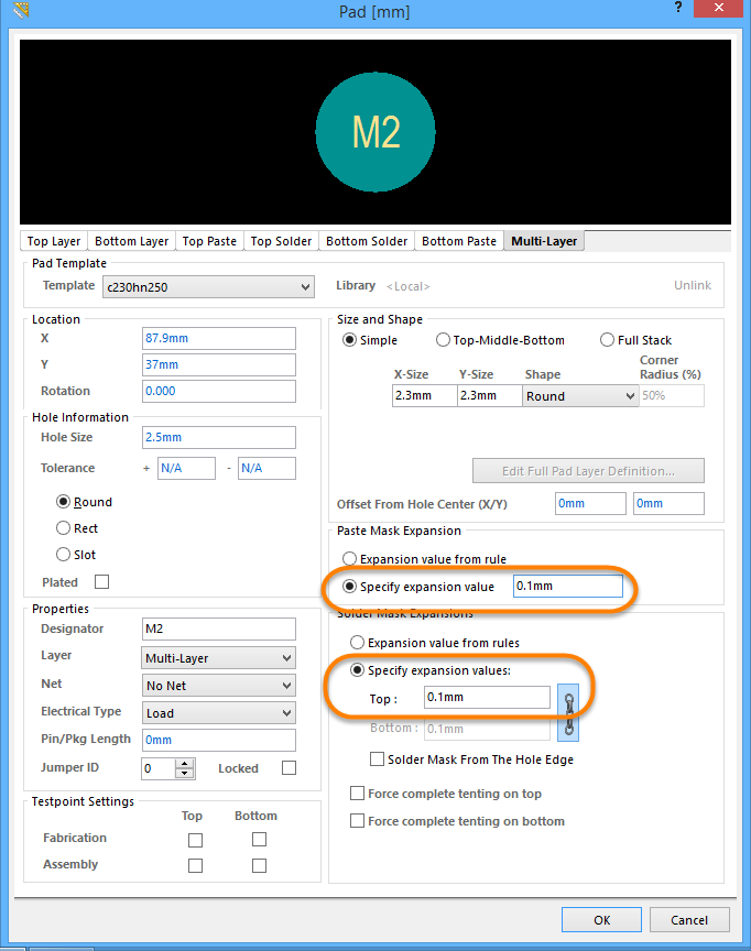
- Type the required value(s) then click OK. Save the footprint.
Designator and Comment Strings
Default Designator and Comment Strings
What you are building in the library is a footprint. When that footprint is placed on a board, it is given a designator and comment and is then referred to as a component. You do not need to manually define placeholders for the designator and comment strings when you build the footprint as these are added automatically when the footprint is placed on a board. The locations of these strings are determined by the designator and comment string Autoposition options in the Component dialog. You can pre-define the required string position (and size) in the PCB Editor - Defaults page of the Preferences dialog.
Additional Designator and Comment Strings
There may be situations where you would like additional copies of the designator or comment strings. As an example, your assembly house wants a detailed assembly drawing with the designator shown within each component outline, while your company requires the designator to be located just above the component on the component overlay on the final PCB. This requirement for an additional designator can be achieved by including the .Designator special string in the footprint (there is also a .Comment special string). To satisfy your assembly house requirement, you would place the .Designator string on a mechanical layer in the library editor, then generate a printout that included this layer. If you need this feature:
- Display the required mechanical layer by enabling the Show and Enable options for each mechanical layer in the View Configurations dialog (Design » Board Layers & Colors).
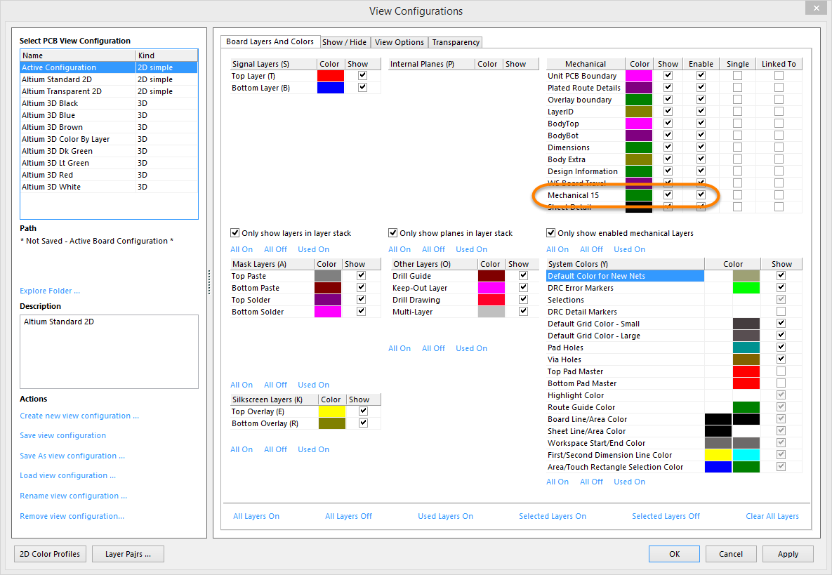
- Click on the Mechanical layer tab at the bottom of the design window to activate this layer. The tab will be highlighted and all new text will be placed on this layer.
- Select Place » String (shortcut P, S) or click on the Place String button.
- Press the Tab key to display the String dialog. Enter ".Designator" in the Properties text box. Set Height to 40mil and Width to 6mil in the diagram then click OK. The bottom left corner of the actual designator will locate where the dot in the .Designator string is located.
- Now we can place the text string. Press the spacebar to rotate the text string, position it in the required location, and click to place it. Right-click or press Esc to exit string placement mode.
- If required, place the .Comment special string using the same procedure.
- To test the special strings, place the footprint on a PCB. You can place the footprint by right-clicking on its name in the PCB Library panel and selecting Place to open the Place Component dialog (assuming a PCB is open). If the designator is not displaying when the footprint is placed in the PCB document, make sure that the Convert Special Strings option is selected in the View Options page of the View Configurations dialog in the PCB Editor.
Handling Special Layer-specific Requirements such as Glue Dots
There are a number of special requirements a PCB component can have, such as needing a glue dot or a peel-able solder mask definition. Many of these special requirements will be tied to the side of the board that the component is mounted on, and must flip to the other side of the board when the component is flipped. Rather than including a large number of special purpose layers that may rarely be used, Altium Designer's PCB editor supports this requirement through a feature called layer pairs. A layer pair is simply two mechanical layers that have been defined as a pair. Whenever you flip a component from one side of the board to the other, any objects on a paired mechanical layer are flipped to the other mechanical layer in that pair. Using this approach, you select a suitable mechanical layer to include the glue dot (or other special requirement) and define its shape using the available objects. When you place that footprint onto a board, you must set up the layer pairing. This instructs the software which layer it must transfer objects to when this component is flipped to the other side of the board. You cannot define layer pairs in the PCB Library Editor; this is done in the PCB Editor.
Including Three-Dimensional Component Detail
Given the density and complexity of today's electronic products, today's PCB designer must consider more than the horizontal component clearance requirements. You must also consider height restrictions and component-under-component placement options. There is also the need to transfer the final PCB to a mechanical CAD tool where a virtual product assembly can verify the complete packaging of the product being developed. Altium Designer includes a number of features, including realistic 3D visualization, for these different situations.
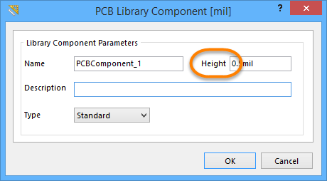
Adding Height to a PCB Footprint
At the simplest level, you can add a height attribute to your footprint. To do this, double-click on the footprint in the Components list in the PCB Library panel to display the PCB Library Component dialog. Enter the desired height for the component in the Height field.
Height design rules can be defined during board design (click Design » Rules in the PCB Editor), typically testing for maximum component height in a class of components or within a room definition.
Adding a 3D Body to a Footprint
For more realistic component rendering in 3D view mode, you can add 3D body objects to the footprint. 3D bodies can be added to a footprint on enabled mechanical layers only. An extruded (simple) 3D body is a 2D polygon-type object that has surface color and a height attribute to pull or extrude the shape when rendered in 3D. 3D bodies can also be created as spheres or cylinders. One or more 3D bodies can be combined to define the physical size and shape of a component in all directions and are used by the Component Clearance design rule. Using high accuracy 3D models improves component clearance checking accuracy and generally improves the visual appeal and realism of the finished PCB assembly. Altium Designer supports directly importing 3D STEP models (*.step or *.stp files) into PCB footprints to render the 3D model. This functionality extends to having STEP models either embedded or linked to Altium Designer PCB documents, however, linked STEP models are not available in the PCB Library Editor.
Manually Placing 3D Bodies
3D bodies can be placed manually in the PCB Library Editor (Place » 3D Body). They can also be added automatically to footprints in the PCB Library Editor (and to placed footprints in the PCB Editor) using the 3D Body Manager dialog (Tools » Manage 3D Bodies for Library/Current Component).
We will now add a 3D body to footprint DIP14, which was created previously in this tutorial. To manually place a 3D body in the PCB Library Editor:
- In the PCB Library panel, double-click the DIP14 entry to open the PCB Library Component dialog. The height of the component is important since we need to make the 3D body representative of the actual height.
- Select Place » 3D Body . After launching the command, the 3D Body dialog (Figure 56) appears. Select the Extruded option in the 3D Model Type region.
- Use the controls in the Properties region to give the 3D body object an identifying name (Identifier), Leave the Body Side (which side of the board the 3D body should project vertically) as Top Side. Note: You can enter a negative standoff height for components that protrude through the PCB, such as pins. Standoff heights are not checked by the Design Rules Checker.
- Define the Overall Height as 200mil and Standoff Height (distance from the board to the underside of the 3D body) to 0mil; set the 3D Color to a suitable color.
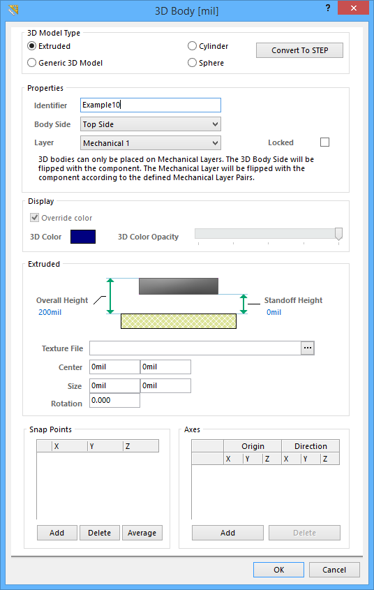
- Click OK to close the 3D Body dialog and enter placement mode. The cursor will change to a cross-hair in 2D, or a blue-cone cursor in 3D.
- Position the cursor and click to anchor the starting point for the body, then continue to anchor a series of vertex points that define the polygonal shape of the body.
- After placing the final vertex point, right-click or press Esc to complete placement of the body. There is no need to "close" the polygon as the software will automatically complete the shape by connecting the start point to the final point placed.
- While defining the shape, use Shift+Spacebar to cycle through various corner modes. Modes available are: any angle, 45°, 45° with arc, 90°, and 90° with arc. Arcs can be increased or decreased in radius using Shift+. (period) or Shift+, (comma), respectively. Use Spacebar to toggle the direction of the corner.
- Use the Backspace key while in placement mode to remove the last placed vertex point. Repeatedly use Backspace to 'unwind' the outline for the polygon back to the initial starting point. You can design and add more 3D bodies for further component detail. After finishing the 3D body, the 3D Body dialog will appear. Continue placing further 3D bodies or click Cancel or press Esc to close the dialog.

DIP-14 3D representation.
- To view the 3D body in 3D at any time, press 3 to enter 3D viewing mode. If you cannot see the 3D body, press L to open the View Configurations dialog and enable the Show Simple 3D Bodies option on the Physical Materials page or use the 3D Bodies Display Options controls on the PCB panel when in 3D Models mode. To return to 2D mode, press 2.
- Save the PCB library.
Interactively Creating 3D Bodies
Interactively creating 3D body objects from a footprint is very similar to the manual method. The basic difference is to use Altium Designer to detect closed shapes that can be used to "extrude" into 3D bodies from the existing objects that comprise the footprint details. This is accomplished through the Component Body Manager dialog.
The Component Body Manager dialog is used to define a 3D body for the transistor package TO-39. Using this approach is easier than attempting to define the shape manually because of the curved shape and orientation tab of the package body. To use the Component Body Manager dialog:
- Make the DIP14 footprint the active footprint in the PCB Library panel.
- Select Tools » Manage 3D Bodies for Current Component to open the Component Body Manager dialog.
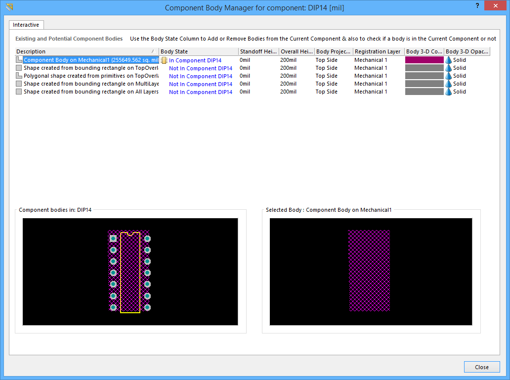
- To create a shape that follows the outline defined on the component overlay, click to select Polygonal shape created from primitives on TopOverlay. Click the entry in the Body State column to add the component, set the Registration Layer to the mechanical layer on which the body object should be placed on (Mechanical 1 in this case), set the Overall Height to a suitable value, and set the Body 3D Color to a suitable color.
- Close the dialog. The 3D body shape will appear on the component. Save the library.
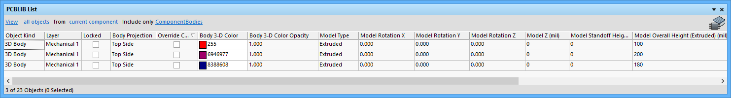
- To edit any 3D body, right-click it and select Properties from the pop-up menu to open the Component Body Manager dialog. You can also use the PCBLIB List panel (shown in the following image) to display 3D bodies and edit them directly.
Importing a STEP Model as a 3D Body
Many component vendors supply detailed 3D models for use in popular mechanical CAD packages. Altium Designer can import 3D STEP models (.step or .stp) directly into a component footprint. This saves time in creating the model yourself and also may provide a more sophisticated model.
Linked STEP Models
Linked STEP models are not supported in the PCB Library Editor. Embedded STEP models are supported.
Importing STEP Models
To import a STEP model, perform the following steps:
- Click Place » 3D Body (shortcut P, B) to open the 3D Body dialog.
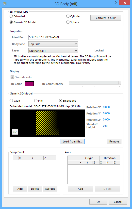
- In the 3D Model Type region, select Generic 3D Model then click the Convert To STEP button.
- In the Generic 3D Model region, select Embedded. Click Load from File to search for and select the desired file.
- Click OK to close the dialog. The 3D body appears floating on the cursor.
- Click in the workspace to place the 3D body object with the selected model loaded into it.
Positioning and Orienting STEP Models
When a STEP model has been imported, the placeholder 3D body re-sizes to house the model. The STEP model may not be oriented correctly in relation to the axes of the PCB document due to the origin used in the originating application. There are several methods for graphically positioning STEP models, using reference points (known as snap points ) placed on the model to manipulate it, and using faces or surfaces on the model in relation to the board. Non-graphical positioning can be carried out through the settings in the Generic STEP Model region of the 3D Body dialog.
Adding Footprints from Other Sources
You can copy existing footprints into your PCB library. The copied footprint can then be renamed and modified to match the specifications required. The following are different ways to copy existing footprints to your PCB library:
- Select placed footprint(s) in a PCB document then copy (Edit » Copy) and paste them into an open PCB library using Edit » Paste Component.
- Select Edit » Copy Component when the footprint to be copied is active in the PCB Library Editor. Change to the open PCB destination library then select Edit » Paste Component.
- Select one or more footprints in the PCB Library panel using standard Shift+Click or Ctrl+Click, right-click then choose Copy. Switch to the target library and right-click in the list of footprint names then choose Paste.
Validating Component Footprints
As in the Schematic Library Editor, there are a series of reports that you can run to check that the footprints have been created correctly and identify which components are in the current PCB library. To validate all components in the current PCB library, run the Component Rule Check report. The Component Rule Check tests for duplicate primitives, missing pad designators, floating copper, and inappropriate component reference. To run the Component Rule Check:
- Save your library file before running any of these reports.
- Select Reports » Component Rule Check (shortcut R, R) to open the Component Rule Check dialog.
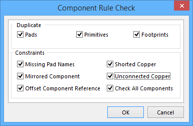
- Check all the boxes available and click OK. A report titled PCB<libraryfilename>.ERR is generated and opens in the Text Editor. Any errors will be noted.
- Close the report to return to the PCB Library Editor.
Creating an Integrated Library
In this tutorial, you have:
- Created an Integrated Library Package - the source project for a compiled integrated library
- Added a new schematic library to the Library Package and created schematic components in it
- Added a new PCB footprint library to the Library Package, created footprints in it and created a 3D model
- Learned how to handle a number of special footprint requirements
The final task is to compile the Library Package to create an integrated library, which creates a single file that includes the components and all their referenced models. Even if we did not want to use the integrated library and prefer to work directly from the source library and model files, there is an incentive to compile the Library Package. Compiling will perform an extensive set of checks on the components and the component-to-model relationships.
To compile the Library Package:
- Compile the source libraries and model files in the library package into an integrated library by selecting Project » Compile Integrated Library. Any errors or warnings found during compilation are displayed in the Messages panel (View » Workspace Panels » System » Messages). Double-click on an error in the Messages panel to view more information and jump to the component. Fix any inconsistencies in the individual source libraries at this point and recompile the integrated library.
- A new Integrated Libraryname.INTLIB is generated, saved in the output folder selected in the Options tab of the Project Options dialog. The new integrated library is automatically added to the installed libraries list and displays in the Libraries panel, ready to use.
For more detailed information about integrated libraries, refer to the Working with Integrated Libraries tutorial.
Glossary
The following terms are used in this tutorial.
|
Component |
A component is a physical device that is placed on the board, e.g., the integrated circuit or resistor. Within these components, there may be either a single part or a set of parts that are packaged together. |
|
3D body |
A 3D body is a polygonal shaped object that can be added to a footprint on any enabled mechanical layer. It can be used to define the physical size and shape of a component in the horizontal and vertical planes, which enables more controlled component clearance checking and better 3D visualization. 3D body objects also act as placeholders for imported STEP models in the component footprint or as non-PCB mounted, free-floating objects, such as housings and assemblies. |
|
Designators |
Designators are unique identifiers that are used to distinguish one component from another in a PCB. They can be alpha, numeric, or a combination of both. Pads also have unique designators that correspond to the component pin numbers. |
|
Footprint |
A footprint defines (or models) the space required by the component to mount it on the PCB. The footprint model of a component is stored in a PCB library. A footprint may contain pads for connecting to the pins of a device and a physical outline of the package created from track and/or arc segments on the silkscreen (overlay) layer. Device mounting features may also be included. Footprints in the PCB library have no designator or comment. They become components when placed on a PCB sheet where the designators and comments are allocated. |
|
Hidden pins |
Hidden pins are pins that exist on the component but do not need to be displayed. Typically, they are power pins and can automatically be connected to a specified net. |
|
Library |
A Schematic Library is a set of components and its parts stored on individual sheets. A PCB Library contains the component footprints. Each library type has its own Editor. Integrated libraries combine schematic libraries with their related models and cannot be edited directly by the Library Editors. |
|
Object |
An object is any individual item that can be placed in the Library Editor workspace. |
|
Pads |
Pads are normally used in a footprint to create connection pads for component pins. |
|
Part |
A part is a collection of graphical objects that represent one part of a multi-device component. Parts are stored in separate sheets within components in the schematic component libraries. |
|
Pins |
Component pins give a component its electrical properties and define connection points on the component. |