Defining Board Regions & Bending Lines
This document is no longer available beyond version 4. Information can now be found using the following links:
Parent page: Rigid-Flex Design
A Board Region is the term used to describe each user-defined area of the board that needs a unique layer stack assigned to it - a standard requirement for a rigid-flex PCB. In the image below the board shape has been divided into three distinct Board Regions: the upper circular region, the thin center strip, and the lower circular region.

A rigid-flex board viewed in Board Planning Mode, note the board shape has been divided into three distinct Board Regions, each showing its region name and the layer stack assigned to it.
When a new board is created it defaults to having a single Board Region. If the board design requires multiple regions, then you can either:
- slice a single Board Region into multiple regions, or
- place multiple Board Regions to build up the overall shape.
► Learn more about Rigid-Flex Design
Working with Board Regions and Bending Lines
Board Regions are Bend Lines are defined and edited in Board Planning Mode (View menu).
There are a number of approaches that can be used to define the Board Regions:
- Interactively place the region - the snap grid, existing placed objects, and user-defined guides can be used to help accurately locate the edges of a Board Region. Learn more about guides and the snap grid system.
- Define the region based on existing design objects - the PCB editor has a number of commands that can be used to define shapes based on an existing outline. The outlines are standard track and arc objects placed on a mechanical layer that are selected, then commands such as Design » Board Shape » Define from Selected Objects can be used to create a Board Region. Learn more about the commands that can be used to convert design primitives into board definition objects.
- Based on detail imported from an MCAD package, such as DXF or DWG - a common approach is for the MCAD engineer to provide the board shape as a DXF or DWG file, which can be imported and used to define the required Board Region(s). Learn more about importing an outline to use to define Board Regions.
- Based on a 3D definition in a STEP file - the MCAD engineer can also provide the board shape as a 3D STEP file which can be used to define the board shape, that shape can then be sliced into separate Board Regions. Learn more about defining the board shape from a STEP file.
Placing a Board Region
A Board Region is a polygonal object, which is placed using the standard polygonal object placement techniques. The board shape must be precisely defined, so it is important that the regions that make up the board are created exactly as required. The video below demonstrates creating Board Regions by aligning their edges against pre-placed workspace guides. The advantage of this technique is that the location of workspace guides can be precisely defined by editing their coordinates in the Properties panel.
Pre-defined workspace guides are used as references for the placement of the Board Regions.
► Learn more about Placing a Board Region
Slicing the Overall Board Outline into Regions
You can divide an existing Board Region into two regions by slicing it. This is done when the PCB editor is in Board Planning Mode.
To slice a Board Region:
- Select View » Board Planning Mode (or press the 1 shortcut) to enter Board Planning Mode.
- Select Design » Slice Board Region (or click the
 button on the Active Bar) to enter Slice Board Region mode.
 - When you select the command you are in slice mode, which is similar to track placement mode. Starting outside of the region to be sliced, click to anchor a series of vertex points that define the slice line. When defining the slice, press Shift+Spacebar to cycle through the corner modes; press the Spacebar to toggle between the Start and End corner modes and use the Backspace key to remove the last placed corner. Place the end of the slice line beyond the edge of the Board Region. When you have finished defining the slice, right-click or press Esc to terminate the command.
- A confirmation dialog opens stating the number of polygons (regions) being split by your action, and the number of polygons (regions) that will be created. Click Yes to confirm their creation.
The board has been split into three Board Regions using the Slice Region command.
Creating Board Regions from Selected Objects
Depending on the shape of your board, it can be more efficient to build up the shape by creating multiple Board Regions. As mentioned above, the regions can be interactively placed, or created by tracing an outline defined from track and arc objects. The video below demonstrates defining three Board Regions from selected objects. In the video you will note that the same object is used to define the adjacent edges where the regions touch, ensuring that these regions are exactly positioned.
A common approach is to define the outline of the regions using tracks and arcs, and then create the Board Regions from the selected outlines.
Modifying the Board Regions
When the PCB editor is configured to operate in the older rigid-flex 1.0 mode, the location where two adjoining regions meet was defined by a movable blue split line. This approach is not used in rigid-flex 2.0, instead, each region is a separate, closed polygonal shape. As a polygonal shape, each region can be adjusted as required using the standard polygonal shape editing techniques. Note that not all polygonal editing commands are available for modifying a Board Region, including the adding and subtracting polygons commands.
Assigning a Layer Stack and Editing the Board Region Name
Related article: Defining the Layer Stack
When a new board is created it will have a single region, named Default Layer Stack Region. This region will be assigned the default layer stack named Board Layer Stack.
When you split a board shape into multiple regions, each new region is also assigned the default layer stack. Once the required layer stacks have been defined in the Layer Stack Manager, then each region can have its stack assigned and also can be given a meaningful name.
To assign a layer stack and name a region:
- Select View » Board Planning Mode or press the 1 shortcut to enter Board Planning Mode.
- Click the Multi-Layer tab at the bottom of the workspace to make it the active layer (if the layer tab is not visible, press L to open the View Configuration panel to enable it).
- Double click on the Board Region to open the Board Region dialog, or single click on the Board Region and open the Properties panel. If the region does not select and the dialog open, make sure that the Selection Filter is not excluding Regions.
- Assign the Layer Stack by selecting the required stack from the Layer stack drop-down.
- Edit the Name as required.
 is also displayed when the assigned stack is configured as flexible.")
The Board Region's Name and assigned Layer stack are displayed in the geometric center of that region. (Flex) is also displayed when the assigned stack is configured as flexible.
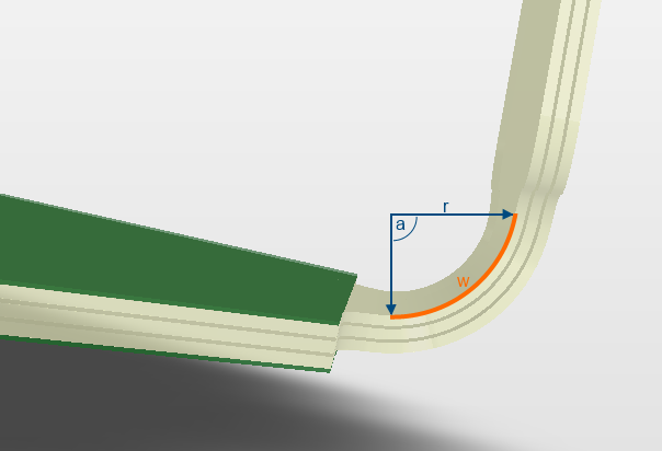
Placing, Positioning and Editing a Bending Line
To define how a flex board should bend, you place one or more Bending Lines. The Bending Line defines where on the surface of the flex region that the bend is to take place. The Bending Line also defines the angle and radius of the bend. The width of the strip of board surface that is being bent is displayed in orange, this width is calculated from the bend angle and radius (learn more about the bending line properties). Bending Lines are placed and edited with the PCB editor in Board Planning Mode (View » Board Planning Mode, or press the 1 shortcut).
Placing a Bending Line
To place a Bending Line:
- Select View » Board Planning Mode or press the 1 shortcut to enter Board Planning Mode.
- Select the Place » Define Bending Line command, or click the
 button on the Active Bar.
 - Click on the edge of the Board Region that you want the Bending Line to cross, move the cursor to the other edge of the Board Region and click a second time. The Bending Line is now placed.
- The cursor remains a cross-hair, ready to place a second Bending Line. Right-click or press Esc if you are finished placing Bending Lines.
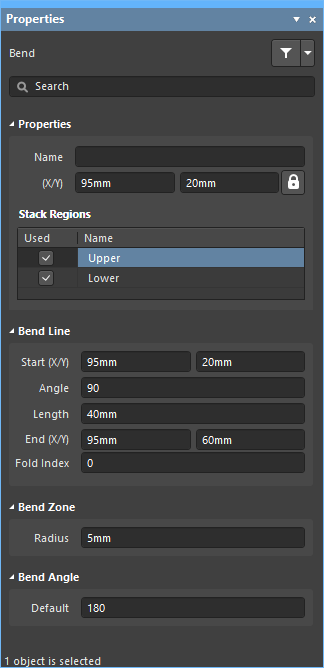
The properties of a selected Bending Line can be edited in the Properties panel. Because the Bending Line is on top of a region, you might find that when you click on the Bending Line the region underneath it selects instead. Without moving the cursor, click a second time to select the Bending Line instead of the Board Region.

The properties of the selected Bending Line are displayed in the Properties panel.
Moving a Bending Line
To modify the location of an existing Bending Line:
- To select a Bending Line, click anywhere within the orange band that defines the Bending Line. The Bending Line will highlight in the current selection color (the default is white).
- Click and hold on the Bending Line handle, move it to the new location, then release the mouse button.
Precisely Locating a Bending Line
When the handle of a Bending Line is moved the handle will snap in accordance with the current snap settings. Press Ctrl+E during movement to pop up the snap setting interactive control panel, as shown in the image below. Press Esc after changing settings to apply the settings and close the panel.
As well as snapping to the snap grid and workspace guides, the Bending Line can also be snapped to existing design objects, such as lines on a mechanical layer. The image below shows a Bending Line handle being positioned on the end vertex of a line on a Mechanical layer. Note that the current Hotspot Snap setting applies (shown on the Status bar) during movement, if the mechanical layer is not the active design layer Hotspot Snap must be configured to All Layers for this snap behavior to work. Press the Shift+E shortcut to cycle the Hotspot Snap setting through the available modes, as you work.

The handle of a Bending Line is being snapped to the vertex of a track placed on a mechanical layer.
Removing a Bending Line
To delete a Bending Line, click anywhere within its orange band to select it, then press the Delete key.
Configuring the Bending Line Properties
To edit the properties of a Bending Line in the Properties panel:
- Switch to Board Planning Mode (press 1).
- Click anywhere within the orange band of the Bending Line to select it.
- The Bending Line can be edited in the Properties panel.
► Learn more about the Bending Line properties.