
Layer Stack Table
Parent page: PCB Objects

A Layer Stack Table can be placed on a PCB document alongside the design itself. It provides a detailed summary of the board layer stackups and how the layer groups are assigned.
Summary
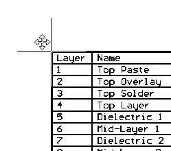
A Layer Stack Table is a tabular graphic object that documents the layers, materials, thicknesses, and dielectric constants implemented in the current PCB design. It is placed and positioned alongside the board design in the workspace and also includes a graphical key and option map that shows the layer stack used in each region of the board. A Layer Stack Table is an important documentation asset for designs with a complex layer stack structure, such as a rigid-flex design.
Availability
The Layer Stack Table is available in the PCB editor when the workspace view is set to normal 2D mode (shortcut 2). It is available for placement in the following ways:
- Choose Place » Layer Stack Table from the main menus.
- Right-click in the workspace then choose Place » Layer Stack Table from the context menu.
Placement
After launching the command, the cursor will change to a cross-hair and you will enter Layer Stack Table placement mode. Placement is made by performing the following sequence of actions:
- Click to place the table.
- The editor remains in Layer Stack Table placement mode, ready to place another table if required. If not, right-click or press Esc to exit placement mode.
Additional actions that can be performed during placement while the layer stack table is still floating on the cursor and before the center point of the layer stack table is anchored are:
- Press the Tab key to pause the placement and access the Layer Stack Table mode of the Properties panel from where its properties can be changed on-the-fly. Click the workspace pause button overlay (
 ) to resume placement.
 - Press the Alt key to constrain the direction of movement to the horizontal or vertical axis, depending on the initial direction of movement.
- Press the Spacebar to rotate the layer stack table counterclockwise or Shift+Spacebar for clockwise rotation. Rotation is in increments of 90°.
Graphical Editing
To move a Layer Stack Table, click, hold and drag the table to the desired location.
Select and drag to reposition a Layer Stack Table.
To remove a Layer Stack Table, select it then press the Delete key.
Non-Graphical Editing
The following methods of non-graphical editing are available:
Editing Via the Properties Panel
Properties page: Layer Stack Table Properties
This method of editing uses the associated Properties panel mode to modify the properties of a layer stack table object.

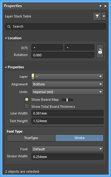
The Layer Stack Table mode of the Properties panel
During placement, the panel can be accessed by pressing the Tab key.
To access the properties of a placed layer stack table:
- Double-click anywhere on the layer stack table object.
- Right-click on the layer stack table then select Properties from the context menu.
- If the Properties panel is already active, click anywhere on the layer stack table object to select it.
Editing Multiple objects
The Properties panel supports editing multiple objects, where the property settings that are identical in all currently selected objects may be modified. When multiples of the same object type are selected manually, via the Find Similar Objects dialog or through a Filter or List panel, a Properties panel field entry that is not shown as an asterisk (*) may be edited for all selected objects.
Via the PCB List Panel
The PCB List panel allows you to display design objects from one or more documents in tabular format, enabling quick inspection and modification of object attributes. When used in conjunction with the Filter panel, it enables the display of just those objects falling under the scope of the active filter – allowing you to target and edit multiple design objects with greater accuracy and efficiency.