
PCB_Dlg-EditRuleFromSchematicEdit PCB Rule (from Schematic) _AD
Created: 七月 14, 2017 | Updated: 二月 27, 2018
| Applies to versions: 18.0, 18.1, 19.0, 19.1, 20.0, 20.1 and 20.2
您正在阅读的是 18.0. 版本。关于最新版本,请前往 PCB_Dlg-EditRuleFromSchematic((Edit PCB Rule (from Schematic) ))_AD 阅读 21 版本

 dialog: Max-Min Width, Routing Layers, Solder-Mask Expansion, and Clearance Rules.")
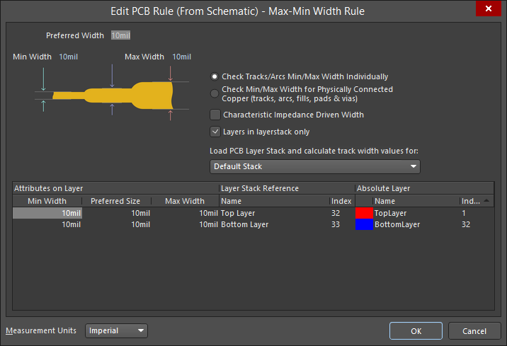
![]() A few variations of the Edit PCB Rule (From Schematic) dialog: Max-Min Width, Routing Layers, Solder-Mask Expansion, and Clearance Rules.
A few variations of the Edit PCB Rule (From Schematic) dialog: Max-Min Width, Routing Layers, Solder-Mask Expansion, and Clearance Rules.
Summary
The Edit PCB Rule (From Schematic) dialog allows you to define the constraints for a PCB rule from a schematic document.
Access
The dialog is accessed by completing the following steps:
- In a schematic, click on a placed Parameter Set Directive (or click Place » Directives » Parameter Set then press Tab) to open the Properties panel in Parameter Set mode.
- Double-click the desired rule in the Rules region of the panel (or click the Add button and add a rule in the resulting Choose Design Rule Type dialog).
Options/Controls
Image Region (If Displayed)
- Click on the available controls in the image (editable measurements are in blue text) to edit the desired areas. If a table also is displayed in the dialog, the table will automatically update after making changes in the image.
- Select the desired options and use the associated drop-downs adjacent to the image to set the desired constraints(s).
Table Region (If Displayed)
- Click on the data you want to edit then enter the desired data. The image above (if displayed) will automatically update.
Additional Controls
- Measurement Units - use the drop-down to select Metric or Imperial units.