
KB: Convert Gerber/ ODB++ fabrication data back to PCB
Created: March 25, 2021 | Updated: March 08, 2024
Starting in version: 18
Up to Current
Converting Gerber/ODB++ fabrication data back to *.Pcbdoc (in other words, reverse engineering the board design data into Altium) involves reading corresponding fabrication data files into CAMtastic, configuring layer stack and drill pairs, extracting netlist, and finally exporting to PCB editor.
Solution Details
Converting Gerber/ODB++ fabrication data back to *.Pcbdoc involves:
-
Reading in fabrication data files for relevant layers with appropriate layer types assigned/mapped into CAMtastic
-
Configuring layer order and drill pairs
-
Extracting netlist
-
Exporting to PCB editor
1. Layer Type Assignment/Mapping
Gerber/ODB++ fabrication data are read in within a CAMtastic document through Import command.1.1 File » New » CAM Document
1.2 File » Import » Gerber or File » Import » ODB++
1.2 File » Import » Gerber or File » Import » ODB++
1.3 File » Import » Drill (Browse to drill file)
All Gerber layers in the CAMtastic document must be assigned to an appropriate layer type. CAMtastic attempts to automate this for you during Import command, matching the extensions of your Gerbers with those listed in Table » Layer Type Detection dialog, but you should always review the Layers Table for completeness and accuracy.
1.4 Tables » Layers (Assign Layer Type)
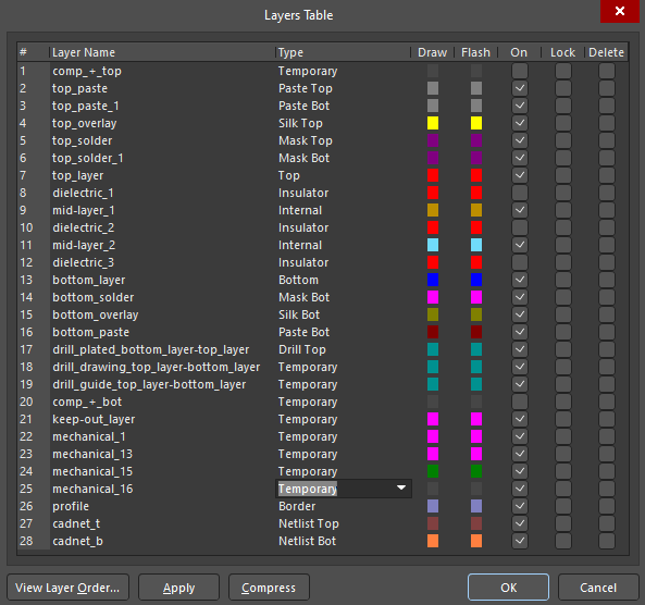
Mechanical layers should be set to Temporary. If you don't have a drill file you can create one by placing a via on a new PcbDoc then export it as NC drill.
2. Layer Order and Drill Pair Configuration
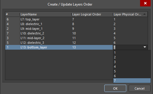
Once all layers are correctly assigned, you should review the Layers Order Table, ensuring that the stack-up of the board is correct.2.2 Tables » Layers Order (Confirm the logical & physical Layer order is correct)
2.3 Tables » Layers Sets (ensure your drill span shows up here)
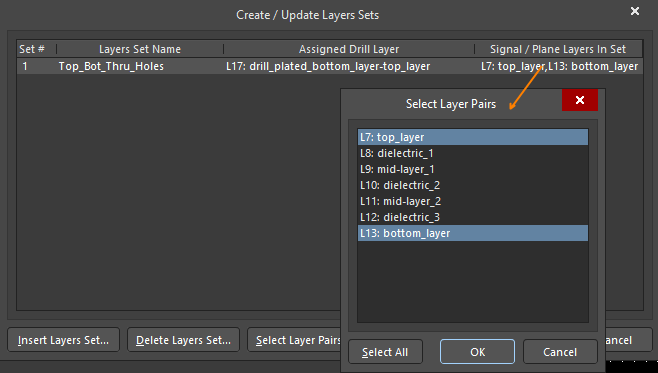
Press and hold CTRL key and click to select a drill pair of start/stop layers.
3. Netlist Extraction
At this point, you may extract a netlist from the CAMtastic file, as this will trace nets from one layer to another according to the layer stackup and drill-pairing sets you have provided.3.1 Tools » Netlist » Extract
If you included IPC netlist files with your Gerber and NC Drill files, you may restore the original net names. An IPC netlist will also differentiate between through-hole vias and free pads in your new PCB file.
4. Export to PCB Editor
The final step is to export the data to PCB editor (*.pcbdoc) where further manual repairing may be required.4.1 File » Export » Export to PCB
All split planes must be defined by closed polylines on the internal plane layers. Island planes may have their borders converted to a closed polyline by joining, but split planes that share their outlines with other splits or with the pullback traces along the board edge must be redrawn. Nested planes such as islands within split planes are not supported by the CAMtastic Export to PCB, but they are supported in Altium Designer's PCB editor. You will simply need to reassign the correct nets to island split planes once you finish the Export from CAMtastic.
In conclusion, CAMtastic’s Export to PCB function will create a board very much like the original. To truly rebuild a board will still take some manual labor, such as replacing primitives with footprints, simply copy and paste groups of primitives into a PCB library, then replace the originals with the new footprints. Additionally, the Layer Pairs in the Layer Stack Manager, should they be required, have to be redefined manually.
If you are working with a footprint Gerber, then you may try opening it in Altium Designer, and perform:
File » Export » DXF
Then open the PcbLib (File » Import » AutoCAD) or PcbDoc (perform File » Import » DXF/DWG)
Please refer our online manual also for this topic:
https://www.altium.com/documentation/altium-designer/cam-editor-reverse-engineering-pcbs-ad