
KB: Cannot select a specific object in PCB to copy, delete, or modify
If there is a specific object in PCB that cannot be copied, deleted, or modified, it may be due to several filtering/locks that prevent a object from being selected and modified inadvertently
Solution Details
If you have a trouble selecting an object in pcbdoc with a mouse click:
- Check your configuration in Selection Filter under Properties panel
- Make sure the board is not currently masked / filtered, press by SHIFT+C to exit the post selection filter mode
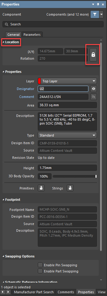
- If the object is of a component footprint locked to the location, double-click to select, after which you can confirm the lock icon button in Properties panel, on General tab, under Location section.
- If the object is a child primitive of the component footprint, Primitives lock icon may need to be toggled to unlock them additionally so it can be selected independently.
- If such primitive is on a mechanical layer that need to be copied exclusively, it would need to be exploded as a free pimitive first by a command Tools » Convert » Explode Component to Free Primitives, after which the primitive can be selected and copied to the clipboard, but be sure to undo the command, so the footprint is put back together as a single component footprint.
- It is also important that the layer on which the object reside is active at the bottom tab
- If all else fails, you may want to leverage PCB Filter and PCBL List panel to interrogate the object parametrically.
Selection Filter (Pre-Filtering)
-
Click the Panels button at the bottom right of the design workspace, then click Properties, to open the Properties panel
-
Note 'Board' at the top left, which implies that there is nothing selected currently in the editor, and check Selection Filter section to make sure object(s) you want to select is highlighted
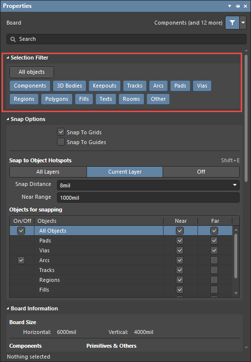
Object Masking (Post-Filtering)
Make sure the board is not currently masked / filtered, press SHIFT+C
Futher details on object masking can be found at:
https://www.altium.com/documentation/altium-designer/pcb-panel#!setting-the-visual-filtering
Locked Component
- If the object is of a component footprint locked to the location, double-click to select after which you can confirm the lock icon button in Properties panel, on General tab, under Location section.
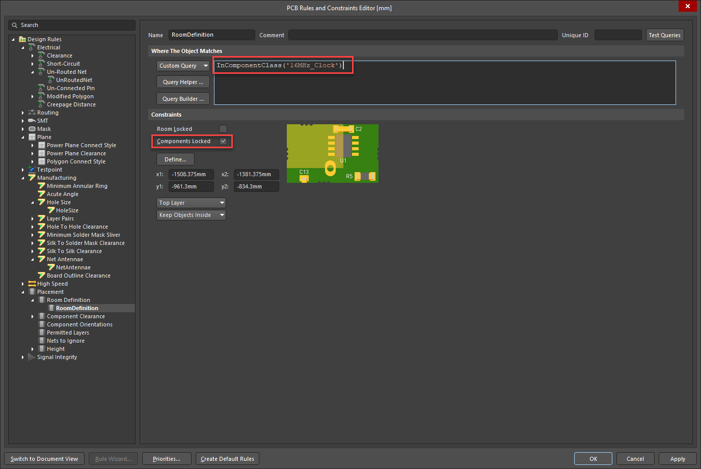
- If the component is unlocked in the properties panel and still requires a double-click to select it, it may be locked by a room in the PCB. To confirm this, check in your design rules for any “Room Definition” rules (Design » Rules » Placement » Room Definition). If any of your Room Definition rules have the “Components Locked” check-box checked, this is likely the cause of a component being locked. To unlock the components, just un-check the “Components Locked” checkbox, or change the “Where The Object Matches” query to exclude the component that you wished to be unlocked. In the screenshot below, any component in the component class “16MHz_Clock” will be locked.
Child Primitive of a Component
If the object is a child primitive of the component footprint, Primitives lock icon may need to be toggled to unlock them additionally so it can be selected independently:
Child Primitive of a Component on a Mechanical Layer
If such primitive is on a mechanical layer that need to be copied exclusively, it would need to be exploded as a free pimitive first by a command Tools » Convert » Explode Component to Free Primitives, after which the primitive can be selected and copied to the clipboard, but be sure to undo the command (Ctrl+Z), so the footprint is put back together as a single component footprint.
Active Layer
It is also important that the layer on which the object reside is active at the bottom tab. 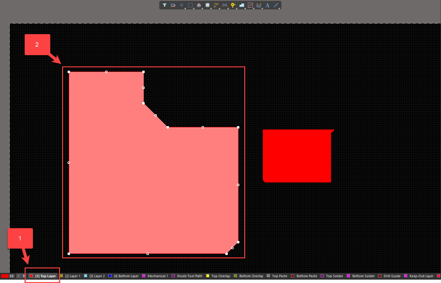
In an event you have multiple objects overlapped one on top of another, you may find 'Display popup selection dialog ' option in Preferences, PCB Editior - General, under Editing Options convenient.
PCB Filter/List Panel
If all else fails, you may want to leverage PCB Filter and PCB List panel to interrogate the object parametrically.
-
To select and remove any debris outside the board in one go that may have come, say, as a consequence of mechanical dxf import.
-
Go to Edit » Select » Outside Area.
-
Make sure that the area you place around your board is as close as possible.
-
Open the PCB List panel.
-
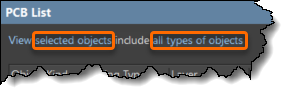
Make sure that the panel is set to selected objects and all types of objects
-
You should only see the objects outside of the board listed in the panel, use Edit » Delete.
-
Futher details on PCB FIlter/List panel can be found at:
https://www.altium.com/documentation/altium-designer/working-with-the-query-language#!pcb_filter_panel