Pin Properties

The Pin Properties dialog
Summary
This dialog allows the designer to specify the properties of a Pin object. A pin is an electrical design primitive. Pins give a component (part) its electrical properties and define the connection points on the part for the incoming and outgoing signals.
Access
The Pin Properties dialog can be accessed prior to entering placement mode, from the Schematic – Default Primitives page of the Preferences dialog. This allows the default properties for the pin object to be changed, which will be applied when placing subsequent pins.
During placement, the dialog can be accessed by pressing the Tab key.
After placement, the dialog can be accessed in one of the following ways:
- Double-clicking on the placed pin object.
- Placing the cursor over the pin object, right-clicking and choosing Properties from the context menu.
- Using the Edit » Change command and clicking once over the placed pin object.
Logical Tab

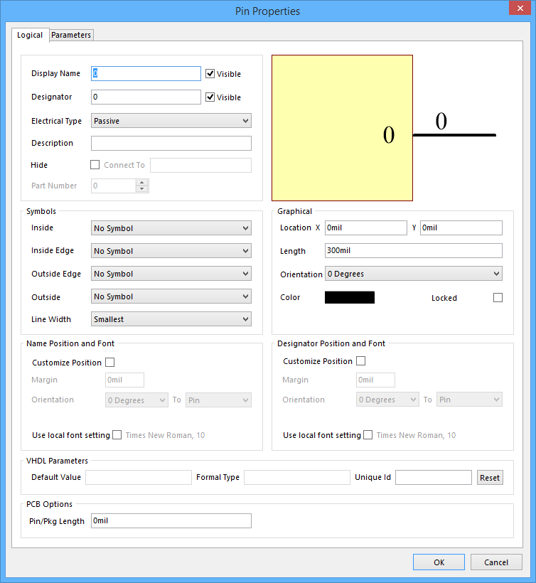
The Logical tab of the Pin Properties dialog
Use the dialog's Logical tab to modify electrical and graphical properties of the pin object.
Options/Controls
- Display Name - use this field to specify an optional display name for the pin. By default, a newly placed pin will be named using the designator value. Supplying a display name is particularly useful for IC-type components, where
the provision of a meaningful name enables a designer to quickly see what the pin is being used for. Note that while the pin name is optional, it is required when the pin is going to be hidden. A hidden pin is automatically connected to other
hidden pins with the same name, and to nets with the same name, when a net-list is created.
- Visible -use this option to determine whether the Display Name for the pin is displayed (enabled) or hidden (disabled) when the parent part is placed on a schematic sheet.
- Designator - the numerical identifier of the pin. Each pin in a part must have a unique designator.
- Visible - use this option to determine whether the Designator for the pin is displayed (enabled) or hidden (disabled) when the parent part is placed on a schematic sheet.
- Electrical Type - use this field to set the electrical type of the pin. This type is used when compiling a project or analyzing a schematic document to detect electrical connection errors (using the Electrical Rules Check feature). Available types are: Input, I/O, Output, Open Collector, Passive, HiZ, Open Emitter, and Power.
- Description - use this field to provide an optional description for the pin, perhaps a concise summary of its purpose.
- Hide - enable this option to hide the pin. This is typically the case for power pins of multi-part components, where their display would otherwise cause unnecessary clutter on the schematic sheet.
- Connect To - use this field to specify the net to which the hidden pin is to be explicitly connected. This is typically a power net, such as VCC or GND.
- Part Number - this field is available when the pin is being added to a multi-part component. Use the associated up/down arrows of the field to specify the part to which the pin is to be associated. A multi-part component also includes a non-graphical part, Part Zero. Part Zero is used for pins that are to be included in all parts of the multi-part component, for example power pins.
- Preview Window - this area of the dialog provides instant visual feedback as you change various options, enabling you to adjust the look and feel of the pin to meet design requirements.
Symbols
Use this area of the dialog to add additional symbols to the pin. Such symbols can be used to visually enhance the component by showing, in a purely graphical way, the electrical characteristic of the pin.
- Inside - use this field to optionally add a symbol to the pin, on the inside of the component graphic. Choose from: No Symbol, Postponed Output, Open Collector, HiZ, High Current, Pulse, Schmitt, Open Collector Pull Up, Open Emitter, Open Emitter Pull Up, Shift Left, and Open Output.
- Inside Edge - use this field to optionally add a symbol to the pin, on the inside edge of the component graphic. Choose from: No Symbol and Clock.
- Outside Edge - use this field to optionally add a symbol to the pin, on the outside edge of the component graphic. Choose from: No Symbol, Dot, Active Low Input, and Active Low Output.
- Outside - use this field to optionally add a symbol to the pin, on the outside of the component graphic. Choose from: No Symbol, Right Left Signal Flow, Analog Signal In, Not Logic Connection, Digital Signal In, Left Right Signal Flow, and Bidirectional Signal Flow.
- Line Width - use this field to determine the width of the line used to draw the symbols. Choose from either Small or Smallest. This provides support for meeting GOST standards, which stipulates that these symbols should be of the same width as the line used to draw the component's symbol.
Graphical
- Location X/Y - the current X (horizontal) and Y (vertical) coordinates for the non-electrical end of the pin (the end that is placed against the component symbol's outline). Edit these values to change the position of the pin in the horizontal and/or vertical planes respectively.
- Length - use this field to specify the length of the pin, in accordance with the currently defined units of measurement.
- Orientation - specify the orientation of the pin, counter-clockwise in relation to the horizontal. Options available are: 0 degrees, 90 degrees, 180 degrees, 270 degrees.
- Color - click the color sample to change the color of the pin, using the standard Choose Color dialog.
- Locked - enable this option to protect the pin from being edited graphically.
Name Position and Font
- Customize Position - enable this option to change from following the default settings for position of the pin's Display Name, to an overriding, customized position.
- Margin - use this field to enter the required margin (space) between the pin's Display Name text and the edge of the component symbol outline.
- Orientation - use this field to choose the orientation of the pin's Display Name text (0 Degrees or 90 Degrees).
- To - use this field to set the reference point for orientation of the Display Name text. Choose from either Pin or Component.
- Use local font setting - enable this option to change from following the default font, to an overriding, customized font, using the font control to the right. This control serves two purposes. Firstly, it reflects the currently chosen font – applied to the pin's Display Name text - in terms of Font Name, Font Size and Font Style. Secondly, when clicked it provides access to the standard Font dialog, from where to change the font as required.
Designator Position and Font
- Customize Position - enable this option to change from following the default settings for position of the pin's Designator, to an overriding, customized position.
- Margin - use this field to enter the required margin (space) between the pin's Designator text and the edge of the component symbol outline.
- Orientation - use this field to choose the orientation of the pin's Designator text (0 Degrees or 90 Degrees).
- To - use this field to set the reference point for orientation of the Designator text. Choose from either Pin or Component.
- Use local font setting - enable this option to change from following the default font, to an overriding, customized font, using the font control to the right. This control serves two purposes. Firstly, it reflects the currently chosen font – applied to the pin's Designator text - in terms of Font Name, Font Size and Font Style. Secondly, when clicked it provides access to the standard Font dialog, from where to change the font as required.
PCB Options
- Pin/Pkg Length - enter the pin-package length. The unit will automatically be entered after you press Enter.
Parameters Tab

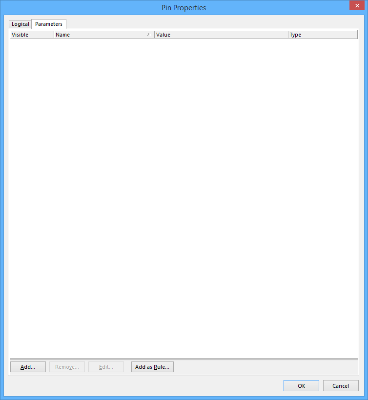
TheParameters tab of the Pin Properties dialog
Use the dialog's Parameters tab to manage parameters attached to the currently selected pin object. You can also add rule-based parameters.
Options/Controls
- Parameters Grid - the main region of the tab lists all of the parameters currently defined for the pin, in terms of:
- Visible - use this option to determine the visibility of the parameter's value in the workspace. Note that this does not relate to the visibility of the parameter's Name, which can be determined, for a standard (non-rule) parameter only, in the Parameter Properties dialog.
- Name - the name of the parameter. For a rule-type parameter, this entry will be locked as Rule.
- Value - the value of the parameter. For a rule-type parameter, the entry will reflect the rule type, along with a listing of its defined constraints.
- Type - the type of parameter, which determines the valid entries that can be used for its value. Available types are: STRING, BOOLEAN, INTEGER, and FLOAT. For a rule-type parameter, this entry is always STRING.
- Add -click this button to add a new parameter to the list. The Parameter Properties dialog will appear. Use this to define the parameter, especially its Name, Value, Type, and whether or not it's value is to be visible in the workspace.
- Remove - click this button to delete the selected parameter(s) from the list of parameters.
- Edit - click this button to modify the currently selected parameter. The Parameter Properties dialog will appear, with which to do so.
- Add as Rule - click this button to add a new design rule directive parameter to the list. The Parameter Properties dialog will appear, but this time will contain the Edit Rule Values button, which in turn gives access to the Choose Design Rule Type dialog, from where you can choose, and subseqently define, the constraints of the required rule type.
Right-Click Menu
The Parameters Grid right-click menu offers the following commands:
- All On - use this command to quickly enable the Visible option for all parameters in the list.
- All Off - use this command to quickly disable the Visible option for all parameters in the list.
- Selected On - use this command to quickly enable the Visible option for all currently selected parameters in the list.
- Selected Off - use this command to quickly disable the Visible option for all currently selected parameters in the list.
- Add - use this command to add a new standard (non-rule) parameter to the list.
- Remove - use this command to remove the currently selected parameter(s) in the list.
- Edit - use this command to edit the currently selected parameter in the list.
- Select All - use this command to quickly select all parameters in the list.
- Select None - use this command to quickly deselect all parameters in the list.
