Working with the Flight Time - Falling Edge Design Rule on a PCB in Altium Designer
Rule category: Signal Integrity
Rule classification: Unary
Summary
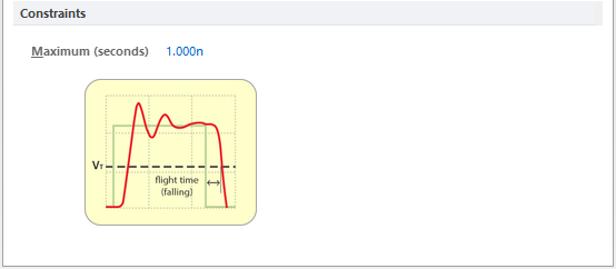
This rule specifies the maximum allowable flight time on signal falling edge. Flight time is the signal delay time introduced by the interconnect structure. It is calculated as the time it takes for the signal on the net to fall to the threshold voltage (marking the transition from signal HIGH to signal LOW), less the time it would take for a reference load (connected directly to the output) to fall to the threshold voltage.
Constraints

Default constraints for the Flight Time - Falling Edge rule.
- Maximum (seconds) - the value for the maximum permissible flight time on the falling edge of the signal.
How Duplicate Rule Contentions are Resolved
All rules are resolved by the priority setting. The system goes through the rules from highest to lowest priority and picks the first one whose scope expression matches the object(s) being checked.
Rule Application
Batch DRC and during Signal Integrity analysis.
