Working with the Polygon Connect Style Design Rule on a PCB in Altium Designer
Created: 6月 05, 2015 | Updated: 9月 26, 2016
| Applies to version: 15.1
現在、バージョン 15.1. をご覧頂いています。最新情報については、バージョン Working with the Polygon Connect Style Design Rule on a PCB in Altium Designer の 21 をご覧ください。
Rule category: Plane
Rule classification: Binary
Summary
This rule specifies the style of the connection from a component pad, or routed via, to a polygon plane.
Constraints
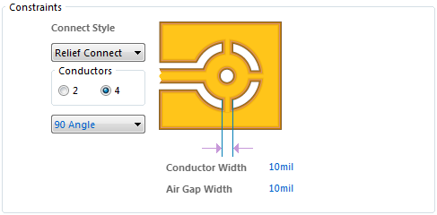
Default constraints for the Polygon Connect Style rule.
Connect Style – defines the style of the connection from a pin of a component, targeted by the scope (Full Query) of the rule, to a polygon plane. The following three styles are available:
Relief Connect– connect using a thermal relief connection.Direct Connect– connect using solid copper to the pin.No Connect– do not connect a component pin to the polygon plane.
The following constraints apply only when using the Relief Connect style:
- Conductors – the number of thermal relief copper connections (2 or 4).
- Conductor Width – how wide the thermal relief copper connections are.
- Angle – the angle of the copper connections (45° or 90°).
- Air Gap Width – the distance between the edge of the pad and the surrounding polygon.
How Duplicate Rule Contentions are Resolved
All rules are resolved by the priority setting. The system goes through the rules from highest to lowest priority and picks the first one whose scope expressions match the object(s) being checked.
Rule Application
During polygon pour.

