Browsing Pad & Via Templates for the Active PVLIB using the Pad Via Library Panel in Altium Designer
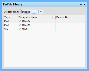
The Pad Via Library panel.
Summary
The Pad Via Library panel provides access to Templates contained in the current Pad Via Library.
Panel Access
When a Pad Via Library Editor is the active document, this panel can be accessed in the following ways:
- Click the
 button in the bottom-right corner of the workspace.
 - From the toolbar, select View » Workspace Panels » PCB » Pad Via Library.
Creating a Pad or Via Template
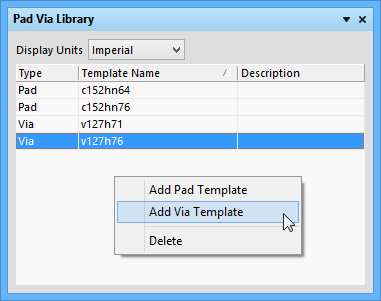
To create a new Pad or Via template, right click within the panel and select Add Pad Template or Add Via Template (respectively) from the associated context menu. Use Delete to remove a template from the Library.
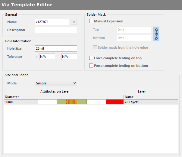
When a new Template is added, the Template editor automatically opens in the workspace. The Pad/Via Template Editor provides the base configuration options for a Pad or Via template which can be applied to a Pad or Via in a PCB or PCB Library document. These include the main properties of a Pad/Via configuration, while document-specific properties are (such its position, orientation, layer, etc) are defined when the Pad or Via is placed in a design document. Saved changes are reflected in the Pad Via Library panel.