
Managing xSignals using the PCB Panel in Altium Designer
This document is no longer available beyond version 21. Information can now be found here: Managing xSignals for version 24
 The xSignals mode of the PCB panel
Summary
The PCB panel allows you to browse the current PCB design using a range of filter modes to determine which object types or design elements are listed, highlighted or selected. The panel also has editing modes for specific object types or design elements that provide dedicated controls for editing procedures. You also can access the properties for any element listed in the panel.
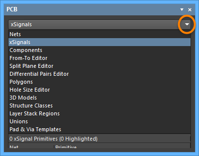
In the PCB panel’s xSignals mode, its three main regions change to reflect the xSignal object hierarchy:
- xSignal Classes
- Individual xSignal definition within a class
- Individual primitives that constitute an xSignal (pads, tracks and vias)
Panel Access
When the PCB Editor is active, click the Panels button at the bottom-right corner of the workspace then select PCB from the context menu. Alternatively, you can access the panel through the View » Panels » PCB command.
Once the PCB panel has been opened, select the xSignals option from the drop-down menu at the top of the PCB panel to enter xSignals mode.
Displaying xSignals in the Workspace
xSignals are displayed in the workspace as a thin line. The line indicates the path that the xSignal follows. The overall length of the line is the X / Y contribution to the signal length of that xSignal. The Z, or vertical contribution to the overall signal length, is described below.
In the image below, the xSignals for a differential pair are shown. The xSignal for the unselected member of the pair remains visible because the checkbox for that xSignal is enabled in the panel.
 xSignals are represented in the workspace by a thin line. Both xSignals in this differential pair remain visible even though only one is selected in the panel because the visibility checkbox is enabled.
Managing xSignals
xSignal Classes Region
The xSignal Classes region lists any xSignal class collections that have been defined or all available classes (<All xSignals>).
Select a class to see its xSignals list in the middle region (xSignals) and to display them in the PCB workspace.
To create a new xSignal class from the existing xSignal collection, right-click in the region then select Add Class from the context menu to open the Edit xSignal Class dialog. The dialog lists the available xSignals that can be added or removed as members to the new class using the management buttons. Use the Name field to define a suitable name for the new xSignal class.
 Create or add to an xSignal class by adding/removing xSignal members using the Edit xSignal Class dialog.
The panel region’s right-click context menu also offers the ability to remove (Delete) or change its visual representation in the PCB workspace (for example, Change xSignal Color).
xSignals Region
The middle region of the panel displays xSignals from the xSignal Class(es) selected in the region above.

The following information is listed with each xSignal by default:
-
 - this feature has two functions:
- color background - the color assigned to the xSignal (the thin line that represents the xSignal in the workspace). Right-click to Change xSignal Color for all currently selected xSignals.
- visibility checkbox - use this to always display the xSignal regardless of whether it is currently selected or not.
- Name - name of the xSignal.
- Node Count - the total number of pads in this xSignal.
- Routed Length - the sum of the lengths of the placed track and arc segments that form the routing plus the vertical distance traversed through vias (see note below). The routed length calculator does not attempt to resolve overlapping track segments or routing wiggles inside pads.
- Signal Length - accurate calculation of the total node-to-node distance. The following notes apply to Signal Length calculations:
- Resolves overlaps and wiggles inside pads.
- Handles routing paths created with objects other than tracks and arcs (e.g., a region or a fill).
- Includes vertical distances through vias (see note below).
- Includes the Total Pin/Package Length for this xSignal.
- Includes the Un-Routed (Manhattan) Length for this xSignal.
- Failure to comply with applicable Length/Matched Length design rules is flagged by the signal length being displayed on a colored background: signal lengths that are too short in yellow, signal lengths that are too long in red.
► See Length Tuning to learn more about how the Length and Matched Length design rules are applied.
- Total Pin/Package Length - the sum of all the Pin Package Length values in all pads in that xSignal. This value is defined as a property of the PCB pad and can also be specified in the schematic pin.
- Unrouted (Manhattan) Length - the vertical plus horizontal (X+Y) distance of all unrouted sections.
Right-click in the region then use the Columns sub-menu to add the following column:
- Delay - the time it takes for a signal to propagate along that route.
xSignal Primitives Region
The PCB panel’s third region, xSignal Primitives, lists all the constituent elements (primitives) of the currently selected xSignal.
Select the region’s Show nodes only checkbox to restrict the primitives listing to pads that are the xSignal start/end point nodes. In this mode, the selected xSignal will be shown in the PCB workspace as node pads joined by a thin trace (rather than tracks) that represents the xSignal path.
 The lower xSignal Primitives region lists all elements of the selected xSignal, such as pads, vias, and tracks and their corresponding delay.
Create xSignals in Nets Mode
While xSignals are generally defined through the Design » xSignals » Create xSignals command, they also can be defined manually using the PCB panel in Nets mode.
As a high-speed connection, we want two nets and series component defined as a one xSignal so it can be used to scope design rules.
When selected in the PCB panel in Nets mode, two nets are highlighted in the PCB workspace.
To create a suitable xSignal, select the source and destination pads in the panel’s Primitives region, right-click on the selection then choose Create xSignal from the context menu. The newly created xSignal will now be available in the PCB panel’s xSignals mode – its default name can be changed by selecting Properties from the right-click context menu. Note that xSignal path incorporates both nets and the series component as a single entity.
► See PCB panel - Nets Mode
► See Defining High Speed Signal Paths with xSignals to learn more about xSignals.