
Using the PDN Analyzer Panel to Drive PDN Analysis in Altium Designer
This document is no longer available beyond version 22. Information can now be found here: PDN Analyzer Interface for version 24
Parent page: Working with Panels
Summary
The PDN Analyzer panel provides the user interface for the Altium PDN Analyzer powered by CST® (Computer Simulation Technology) Power Deliver Network (PDN) analysis tool, available as an Altium Extension application for Altium Designer. The highly configurable tool analyzes a board design's DC performance based on its electrical and physical properties, and thanks to its direct integration into the design software, displays real time network Power Integrity results in the PCB editor using both the 2D and 3D view modes.
► See the PDN Analyzer page for an overview of the DC simulation tool and the principles involved.
► See the PDN Analyzer Example Guide for information on using the tool.
Panel Access
When a PCB project design document is active, select Tools » PDN Analyzer from the main menu to open the PDN Analyzer panel.
► See Installation and Licensing information.
Layout Modes
The dockable PDN Analyzer panel is best used in conjunction with the software's PCB Editor so the visual results of analysis run may be seen immediately in the design's copper layout. In its floating (undocked) mode the panel might be moved to a second monitor to maintain visual access to the PCB Editor, or the panel may be vertically/horizontally docked in the main design screen to share real estate with the PCB Editor.
For the latter case, the panel offers a compact interface mode that moves its main configuration pane to a separate tab option (Config). To switch to this mode, select the Compact Layout option from the panel's  button drop down menu in the configuration pane/tab.
 In Compact Layout mode the Configuration pane changes to tab access, which preserves screen space for the PCB Editor.
Configuration
The Configuration pane (or Config tab) is devoted to simulation network control and presents an interactive graphic representation of the currently selected power network(s).
Simulation and network management
The section on the left of the Configuration pane/tab is used for simulation file management, and provides a hierarchical view of the simulation's loaded power networks. The complete network structure or individual power networks may be selected. The section's options include:
- The drop down menu.
- New Simulation – start a new PDN simulation, based on a single power/ground network.
- Open – open a previously saved or example simulation configuration file (
*.pdna). - Save – save the active simulation configuration to disk as the current name.
- Save As – save the active simulation configuration to disk as the desired name.
- Explore – open a Windows file browser in the location of the active simulation.
- Explore Samples – open a Windows file browser in the location of the installation's example project (stored as a zip archive) – unzip this project to a convenient location. Note that the project also includes a set of example PDN Analyzer configuration files, where each is set to a specific copper temperature; 25°C (nominal), 100°C, 175°C.
- Compact layout – the alternative screen mode outlined above.
- Right click options – accessed by right clicking on the top level simulation name.
- Import (1.x) – load a simulation configuration saved from the previous
1.xxversion of the PDN Analyzer (*.pidc_config). - New Network – create a new base-level network within current simulation configuration.
- Remove – unload the selected simulation.
- Delete – remove the selected network from the simulation (available as a right click option on the name of an individual network).
- Clear Results – reset the power network analysis results, including those cached from a previous simulation run.
- Revert – restore the last simulation analysis results and its corresponding configuration.
- Save – save the active simulation configuration to disk as the current name (
*.pdna). - Save As – save the active simulation configuration to disk as the desired name.
- Copy – clone the selected network simulation.
- Explore – open the
/PDNAnalyzer_Outputfolder for the current simulation in a Windows file browser. Note that this includes a fully detailed event log file for the most recently run simulation (PDNAnalyzer.log). - Settings – opens the Settings dialog for the current simulation configuration. The settings can be exported/imported (
*.pdna.settings) and reset to their defaults.
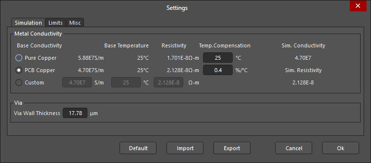
The dialog includes the:- Simulation tab – specify the Metal Conductivity settings for the physical board copper and the weight (wall thickness) of the layer connection Vias.
- Limits tab – specify the maximum current density limits detected by the simulation for both copper layers and Vias of two sizes.
- Misc tab – set simulation parameters such as the applied current density units and data smoothing (Noise Filtering), and voltage offset scheme used to establish the design's zero voltage reference.
- Import (1.x) – load a simulation configuration saved from the previous
- The
 button, which opens the PDN Analyzer DC Net Identification dialog – also opened when the PDN Analyzer is first invoked. The system will attempt to automatically detect suitable DC power nets within the current PCB design.
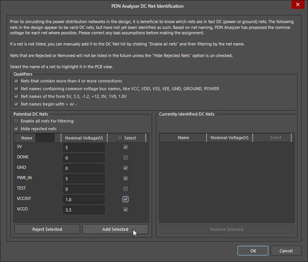
Use the dialog options to help correctly identify the DC nets and their nominal voltage levels.- Qualifiers – deselect qualifier filters if necessary to correctly identify the design's DC nets. The filters are based on number of connection and common power network nomenclature.
- Potential DC Nets – a tabular list of the identified power net in the design. Use the Enable all and/or Hide rejected options to populate the list as needed for your DC power analysis.
- Name – the net name as extracted from the board design's net data. Use the associated search field to filter the listing by an entered key word.
- Nominal Voltage – enter a suitable voltage for power nets as basic source data for the analysis.
- Select – use the checkboxes to nominate which nets would like to be registered (identified) by the PDN simulation.
- Reject/Add Selected – use the
 and
and  buttons to manage which nets are populated into the Currently Identified DC Nets listing.
- Currently Identified DC Nets – a tabular list of power nets that will be available to the PDN simulation, as populated from the Potential DC Nets listing.
- Select – use the checkboxes to select nets that will be removed (moved from the identified nets list back to the potential nets list) by the
 button.
- Select – use the checkboxes to select nets that will be removed (moved from the identified nets list back to the potential nets list) by the
- The
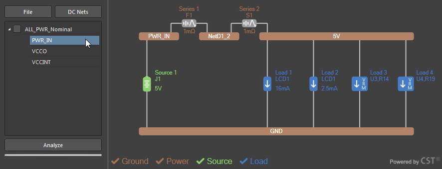
 button, which invokes the power network simulation and analysis routines. This button is enabled when the power network and its related data is fully configured, as indicated by tick icons associated with the Ground, Power, Source and Load labels in the power network diagram graphic.
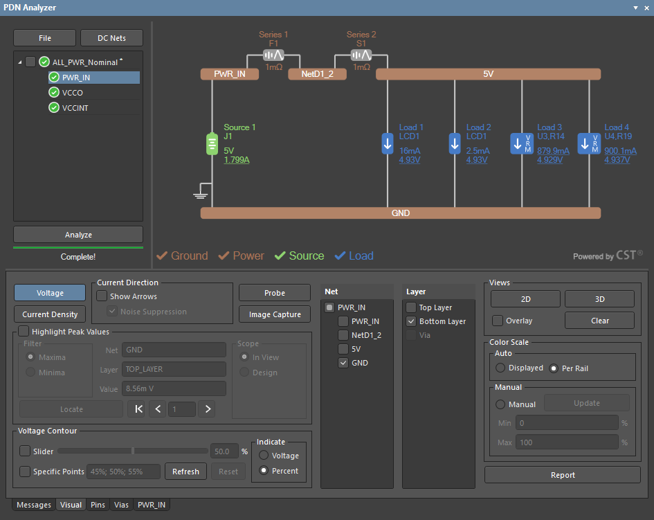
Power Network Graphic
The main body of the Configuration pane provides an interactive graphic representation of the power network structure selected in the simulation's network tree (on the left). When the top level simulation name is selected, the graphic shows the overall connectivity of sub power networks – double click on a sub network graphic element to open that sub network. The interactive graphic also is used to construct a power network from the PCB design's net data and connectivity by using its right-click options, or by double-clicking on graphic elements.
Right click on the configuration graphic or one of its elements to access the following options:
- New Network – create a new base-level network (power and ground nets) within current simulation.
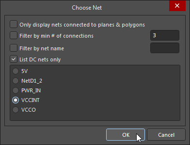
- Edit Net – specify a power network's settings in the Choose Net dialog (also available by double-clicking on a network element). The dialog includes a selectable list of nets available to the simulation (as defined in the PDN Analyzer Net Identification dialog, opened from the button) and several filter options that can be used to constrain the listing.
- Extend Net – use to add another net to the selected net via a series element, which will be inserted automatically. The additional net is selected in the Choose Net dialog, while the inserted series device is configured by double clicking on its element to access the Device Properties dialog. See Extending Networks Through Series Elements for more information.
- Add Source – add a Voltage or Voltage Regulator Model (VRM) source device between a specified power/ground net pair via the Device Properties dialog. The dialog also is available by double-clicking on an existing Source element. See Including Voltage Regulator Models for more information on working with VRMs.
- Add Load – add a Resistor, current sink or Voltage Regulator Model (VRM) load device between a specified power/ground net pair via the Device Properties dialog. The dialog also is available by double-clicking on an existing Load element.
- Delete – remove the power net from the simulation. Note that a network must include one power net and one ground net as a minimum.
- Settings – open the Settings dialog, as outlined above.
The Device Properties dialog, used when adding or editing an existing device element (Load, Source, etc) provides settings to specify the device type, connectivity and parameters.
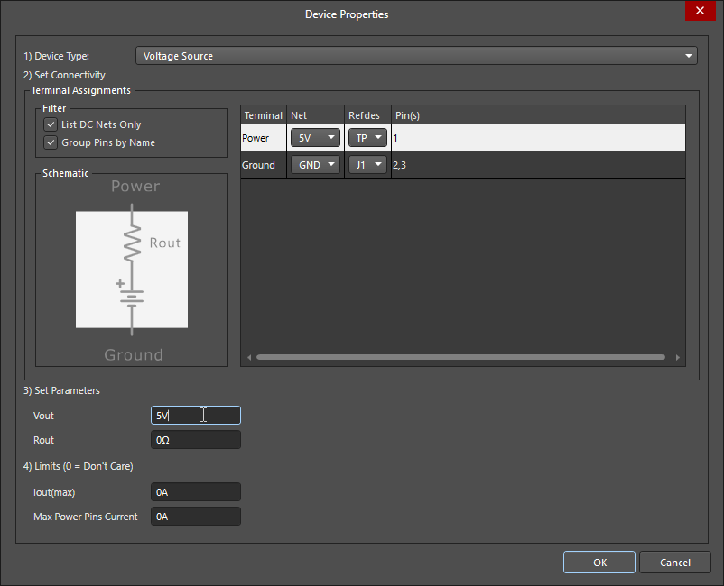
The dialogs's available settings options will depend on the function of the device element being placed or edited, but are generally as follows:
- Device Type – use the drop down menu to select type of device, where the available options are determined by the element type (Source, Load, etc).
- Set Connectivity – use the listing's Net and Refdes dropdown options to choose the device's Terminal connections from the available nets and nodes, where the Terminals are as indicated in the Schematic simulation model graphic. The net connection Pins are automatically assigned based on the specified node's net connectivity.
- Filter – use List DC Nets Only option to constrain the available Net options, and the Group Pins by Name option to combine interconnected device pins. When the latter is disabled, individual pins can be selected/deselected as required using the Select checkboxes exposed by clicking in the Pins field. See the LCD example in Working with Loads for more information.
- Set Parameters – the available parameter options will depend on the type of device being placed (or edited), but generally define its base properties such as the output voltage and internal resistance of a Voltage Source, the load current of a Current sink, or the resistance value of a Resistor load.
- Limits – the device's Voltage, Current or Power limitations that will trigger a Violation when the simulation is run. A violation is indicated by a dashed red border around the graphic of the offending element and a red icon associated with the network name: see Current Density Limit Violations or Other Violations for examples.
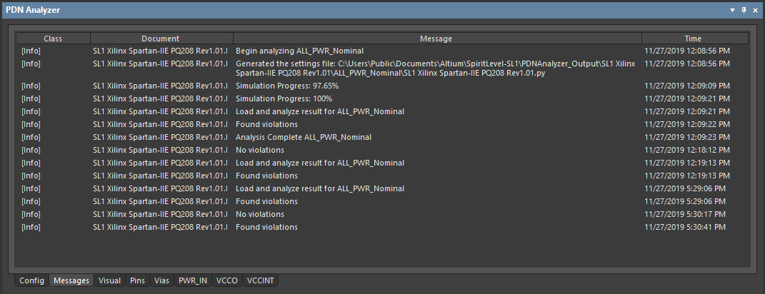
Messages tab
The Messages tab includes a sequential listing of simulation events for the most recently run PDN analysis, including any Violations that were encountered. In the situation of a failed simulation run, the list will include an event entry summarizing the issue. For more information on a simulation run, see the PDN_Analyser.log file available via the configuration Explore option.
Visual tab
The PDN Analyzer interface's Visual tab provides a high level of control over how the power network analysis data is displayed in the PCB Editor. It allows you to specify what type of information is included in PCB layout rendering, the scaling of the results data, how and if points of interest are highlighted, and what information is exported. The rendered layout in the PCB Editor applies to the power network that is currently selected in the PDN Analyzer's Configuration network hierarchy.
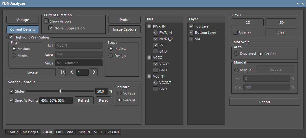
Use the Visual tab's default settings as a starting point for setting up the PCB layout display. These are set to show the color-graduated voltage profile across all power rail nets in 2D mode – deselect the Overlay option to see the pure analysis results. Setting changes made in the Visual tab are immediately reflected in the PCB rendering.
The Visual tab options include:
- Voltage – select the
 button to display the voltage profile across all enabled nets, scaled in Volts or as an overall percentage span (see Color Scale).
 - Current Density – select the
 button to display the current density profile across all enabled nets, scaled in Amps per area or as an overall percentage span (see Color Scale).
 - Current Direction – check the Show Arrows option to overlay current direction/distribution indicator arrows on the rendered PCB layout. Select the Noise Suppression option to apply data smoothing for a less cluttered visual result.
- Probe – select the
 button to open the Probe dialog, where two data locations in the rendered layout can be interactively selected and their numerical values compared. See Data Probe for more information.
 - Image Capture – select the
 button to open the Manage Image Capture dialog, where the current PCB rendering can be captured and saved. The images are stored in the project simulation's
 /HTMLReport/ImagesCachefolder for later inclusion in a Report. See Analysis Report for more information. - Peak Values – select the Highlight Peak Values option to visually mark and highlight the maximum or minimum (as per the Filter options) Value in the currently selected nets and layers. Use the Scope options to specify the detection area, the Locate button visually highlight the peak value point, and the data point arrows (

 ) to step though the adjoining sequence of values. See Locating Power Integrity issues for example information.
 - Voltage Contour – select the Slider option to enable a dashed line overlay which represents the voltage level at that contour line. The detected level is that set by the slider position, and is a voltage or percent value as determined by the associated Indicate options. Select the Specific Points option to enable voltage contour lines at each on the indicated percentage points. Click
 to set the Specific Point values to their defaults, and the
  button to update/highlight all enabled voltage contour lines. See Voltage Contour for more information.
 - Net – select the Nets you wish to display in the rendered PCB analysis results. The nets are grouped by available power networks.
- Layer – select the board Layers you wish to display in the rendered PCB analysis results. Note that Vias are available for selection when in 3D view mode.
- Views – use the
 and
and  buttons to change the rendered display between the PCB Editor's 2D/3D modes, the Overlay option to enable/disable the editor's standard PCB display view, and the
  button to revert the rendered display to the standard view. See Display Control and Options for more information.
 - Color Scale – set the Auto options to show the rendered color gradient as an overall percentage range (Per Rail) or as a gradient that corresponds to the complete voltage span data (Displayed). The latter is best used when a single net is being displayed. Select the Manual mode to override the displayed range to the voltage values entered in the Min and Max fields. See Visual Rendering in the PCB Editor for more information.
- Report – click the
 button to configure and generate an HTML-based PDN Analysis report via the HTML Report dialog. See Analysis Report for more information.
Pins tab
The Pins tab presents a list of all component pins in the design connected to configured power networks. Each component pin entry includes its number, connected net, and the associated Voltage and Current value results from the last simulation run. Click on a column header to order the list by that name, and click again to reverse the order.
Double click on an entry to cross probe to that pin in the PCB Editor. If the pin (pad) connection cannot be seen in the rendered view, ensure that the Layer and power Net it is connected to are enabled in the Configuration pane/tab.
 The Pins tab listing ordered by Component reference and – hover the cursor over the image – ordered by pin Current.
Vias tab
The Vias tab presents a list of all PCB vias in the design connected to configured power networks. Each via entry includes its connected net, location co-ordinates, layer pair, and the associated end-to-end Voltage, Current and Current Density value results from the last simulation run. Click on a column header to order the list by that name, and click again to reverse the order.
Double click on an entry to cross probe to that via in the PCB Editor. If the via cannot be seen in the rendered view, ensure that Via is checked in the Layer list (available in 3D view) and its connected power Net is enabled in the Configuration pane/tab.
 The Vias tab listing ordered by Net connection and – hover the cursor over the image – ordered by Current Density.
Power Network tabs
A tab view is available for each available power network within the simulation configuration – the network tabs that are visible is determined by the power network selection in the Configuration pane/tab. Labeled as the network name, the power network tab provides a comprehensive listing of grouped simulation results and calculated data that applies to that power network. A network power consumption summary is also included.
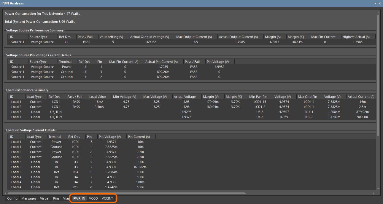
The data groups in the listing apply to devices within the power network (sources, loads, and series elements), where a Performance Summary and a Pin Voltage/Current Details data entry is included for each device. Along with details about the device, the data groups present key voltage and current values, and in the case of the Performance summary, calculated safety margins that relate to the device limits as specified in the Device Properties dialog.