
Working with a Board Region Object on a PCB in Altium NEXUS
Parent page: PCB Objects
, which run from one edge of the board shape to another edge.") A board is split into distinct regions by placing Split Lines (blue in color), which run from one edge of the board shape to another edge.
A board is split into distinct regions by placing Split Lines (blue in color), which run from one edge of the board shape to another edge.
Summary
A Board Region is a user-defined area of a PCB that can have a unique layer stack assigned to it. A board can be split into multiple regions by placing one or more Split Lines, dividing its single default region into multiple regions. Each region can then be assigned an individual layer stack. The layer stackups can be configured to cater for both rigid and flexible regions of the board, facilitating rigid-flex PCB design.
Availability
Board Regions can only be implemented in the PCB Editor with the View mode set to Board Planning Mode (View » Board Planning Mode – press the 1 shortcut).
The region sections are defined by placing Split Lines (Design » Define Split Line), which segment the board outline shape. A single board region (for example, that of a newly-created board) is split into two regions by placing a Split Line.
Placement
Board Regions are defined by placing Split Lines to divide an existing board region into smaller regions:
- Select View » Board Planning Mode (or press the 1 shortcut) to enter Board Planning Mode.
- Select Design » Define Split Line to enter Split Line placement mode.
- Click within the board shape to begin the Split Line definition process. One end of the line will attach to the closest point on the board shape outline to where you clicked, the other end of the line will attach to the cursor.
- Position the cursor in the required location then click once to place the second end.
- You remain in Split Line placement mode, ready to place another Split Line if required. If not, right-click or press Esc to exit Split Line placement mode.
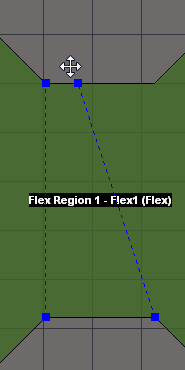
Board Regions are the areas between the Split Lines, and are assigned a default region name.
When a new board is created it will have a single region, and this region will be assigned the default layer stack, named Board layer stack. When the board shape is split into multiple regions, each new region is also assigned this default main layer stack. Each board region is also given a default name, with the original region named Default Layer Stack Region, and subsequent regions named using the format Layer Stack Region.
Graphical Editing
Within a board layout, Board Regions are defined by the positioning of Split Lines. The Split Line can be graphically edited by manipulating the nodes at the end of each line using a select and drag method.
To edit a Board Region by moving a Split Line:
- Select View » Board Planning Mode (or press the 1 shortcut) to enter Board Planning Mode.
- To relocate the end of a line, click, hold and drag it to the required location around the perimeter of the board shape. The cursor will be constrained to the current snap grid.
- The Board Region will be redefined by the new position of the edited Split Line.
 Select and drag a Split Line end
node to redefine a Board Region
area.
To redefine a Board Region by removing a Split Line:
- Select View » Board Planning Mode (or press the 1 shortcut) to enter Board Planning Mode.
- Click and hold the split line by one of its end points, then press the Delete key. Alternatively, click, hold and move an endpoint to a point around the board shape that results in the split turning red (signifying an invalid split), then release.
Non-Graphical Editing
The following methods of non-graphical editing are available:
Editing Via the Properties Dialog
A Board Region's properties can be accessed and edited from the Board Region dialog, which is opened by double-clicking on the region. Note that the PCB editor should be in the Board Planning Mode view – View » Board Planning Mode (shortcut 1).
 The Board Region dialog
To give a region a more meaningful name, update the Name field in the Board Region dialog. Similarly, to assign the required layer stack to the selected region, select the appropriate layer setup from the layer stack list. Note that one board region must have the 3D Locked option enabled to define the physical ground reference for the 3D display mode.
Click OK to accept the new setting and close the dialog.
Editing Via the PCB Panel
The PCB panel allows you to browse the current PCB design using various filter modes to determine which object types or design elements are listed, highlighted or selected. It also has editing modes for certain object types or design elements that provide you with specific controls on the panel for editing procedures.
Set the PCB panel browsing mode (top drop-down list) to Layer Stack Regions. The panel shows:
- The available board layer stacks in the Layer Stacks list area.
- The Regions assigned to those stacks in the Stackup Regions list area.
- Any bending lines defined in the selected Region in the Bending Line list area – see Bending Line for more information.
To edit the properties and elements of a selected Board Region:
- Double-click on a region in the Stackup Regions list to open the Board Region dialog.
- Double-click on a bending line in the Bending Lines list to open the Bending Line dialog.