Pads are available for placement in the PCB editor in the following ways:
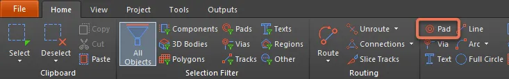
- Choose Home | Place | Pad from the main menus.
After launching the command, the cursor will change to a crosshair and you will enter pad placement mode.
- Position the cursor then click or press Enter to place a pad.
- Continue placing further pads or right-click or press Esc to exit placement mode.
A pad will adopt a net name if it is placed over an object that is already connected to a net.
Additional actions that can be performed during placement are:
- Press the Tab key to pause the placement and access the Pad mode of the Inspector panel in which its properties can be changed on the fly. Click the design space pause button overlay (
 ) to resume placement.
- Press the Alt key to constrain the direction of movement to the horizontal or vertical axis depending on the initial direction of movement.
Graphical Editing
Pads cannot have their properties modified graphically other than their location.
- To move a free pad and also move the connected tracks, click and hold then move the pad. The connected routing will remain attached to the pad as it is moved.xxx
- To move a free pad without moving the connected tracks, choose Tools | Arrange | Move » Move Object, click and hold then move the pad.
If you click and drag a selection rectangle around component pads, they will not select as they are actually child objects of the component. To subselect just the pads, hold Ctrl as you click and drag the selection window.
To clear the selection of (or de-select) the object, use the Esc key.
Non-Graphical Editing
This method of editing uses the Inspector panel to modify the properties of a Pad object.

During placement, the Pad mode of the Inspector panel can be accessed by pressing the Tab key. Once the Pad is placed, all options appear.
After placement, the Pad mode of the Inspector panel can be accessed in one of the following ways:
- If the Inspector panel is already open, select the Pad object.
- With the pad selected, choose View | Schematic | Inspector from the main ribbons.
Press Ctrl+Q to toggle the units of measurement currently used in the panel between metric (mm) and imperial (mil). This only affects the display of measurements in the panel; it does not change the measurement unit specified for the board, which is configured in the Units setting in the Inspector panel when there are no objects selected in the editing design space.
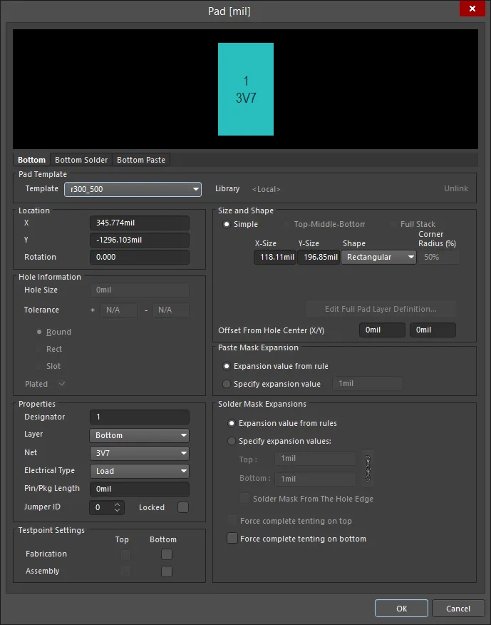
Pad Dialog
Pad properties can also be changed using the Pad dialog, which is accessed by clicking the Edit button under the Pins in Focused Net region in the Netlist Manager dialog (Tools | Netlist | Neliist » Edit Nets).
To toggle the units of measurement used in the dialog between metric (mm) and imperial (mil), press Ctrl+Q.
Layer Selection - click the layer tab to view the desired layer.
Pad Template
- Template - select a Pad template from the drop-down.
- Library - displays to which library the Pad template is linked and includes the option to unlink the template from that library.
Location
Values can be defined in either mm or mil units. When entering a value in units other than the current units, add the mm or mil suffix to the value.
- X - the current X position of the center of the pad relative to the current origin. Edit the value to change the position of the pad relative to the origin.
- Y - the current Y position of the center of the pad relative to the current origin. Edit the value to change the position of the pad relative to the origin.
- Rotation - the current pad rotation in degrees. Edit to change the rotation of the pad. Minimum angular resolution is 0.001°.
Hole Information
- Hole Size - the current hole size for the pad. The value specifies the diameter of the hole (in mils or mm) to be drilled in the pad during fabrication. For a single-layer pad (such as an SMD pad or edge connector), this is automatically set to zero. The hole size can be set from 0 to 1000mil and can be set larger than the pad area to define copper-free mechanical holes. Edit the value in this field to change the pad hole size.
- Tolerance - Setting the hole tolerance attribute can help determine the fits and limits of your board. Specify the minimum (-) and maximum (+) hole tolerance for the design.
Choose one of the following options to specify the shape of the hole:
- Round - specifies a round hole shape (default) for the pad.
- Square - specifies a square (punched) hole shape for the pad.
- Slot - specifies a round ended slotted hole shape for the pad.
- Plated - this option determines whether or not the pad has a plated hole. If both plated and non-plated pads exist in a design, the non-plated holes will be set to use different tools from the plated holes in the NC Drill files.
Separate drill files (NC Drill Excellon format 2) are generated for each hole kind (Round, Square and Slot) as well as for plated and non-plated holes (as defined by the Plated checkbox). This means there can be up to six different drill files generated.
Properties
- Designator - the current pad designator. If the pad is part of a component, the designator is usually set to the corresponding component pin number. The designator can be up to 20 characters in length and cannot include any spaces. Free pads can include a designator or the field can be left empty. If the designator begins or ends with a number, the number will auto-increment when placing a series of pads sequentially. Edit the value in this field to change the pad designator. Note that multiple pads within the same component footprint can share the same designator if required.
- Layer - the layer to which the pad is currently assigned. Pads can be assigned to any available layer, Set the Layer to
Multi-Layer to define a pad shape on all signal layers.
- Net - the net to which the pad is currently assigned. Change the net assignment by clicking in the field and choosing a net from the drop-down list. Select No Net to specify that the pad is not connected to any net. The Net property is used by the Design Rule Checker to determine if a PCB object is legally placed.
- Electrical Type - this field displays the current electrical status of the pad. This status is only relevant for component pads and sets the transmission line characteristics for these pads. Pads can be designated as a Load, Source or Terminator. The Source and Terminator settings are used when a net requires one of the Daisy chain routing topologies. Click the field to change the electrical type from the drop-down list.
- Pin/Pkg Length - the Pin Package Length is automatically included in the Signal Length calculations that are displayed in the PCB panel. Set the PCB panel to Nets mode to examine or edit the value of the Pin/Pkg Length for the pins in the chosen net.
- Jumper ID - set this to a non-zero value (range of 1-1000) to indicate that this pad is part of a jumper component footprint. Jumper components can be used on a single-sided PCB when there will be a wire link that physically connects the pads together rather than using tracks to create the connection. The Jumper ID value tells the software which pads to treat as 'connected'. A jumper connection can only be created between the pads within the same component footprint; they must have the same Jumper ID value and must also be assigned the same net. The component must also have its Type set to Jumper. When these conditions are met, a jumper connection is shown as a curved connection line in the PCB editor.
- Locked - enable to protect the pad from being edited graphically. Lock a pad whose position or size is critical. If you try to edit a primitive that is locked, you will be informed that the primitive is locked and asked if you want to proceed with the action. If this option is unchecked, the primitive can be freely edited without confirmation. Note that the Locked checkbox has no effect on a pad that belongs to a component. If the component is not locked, the pads will move when the component is moved. In this situation, lock the component to prevent accidental movement.
Testpoint Settings
Use this region to define this pad as a testpoint for Fabrication and/or Assembly testpoint file generation. A testpoint is a location where a test probe can make contact with the PCB to check for correct function of the board. Any pad or via can be nominated as a testpoint. When this is done, the component to which the pad or via belongs automatically gets locked.
- Top - enable this option for this pad to be defined as a top layer testpoint.
- Bottom - enable this option for this pad to be defined as a bottom layer testpoint.
Size and Shape
The copper area (land area) of the pad is defined by the X and Y Size and the Shape settings.
- Simple - a simple pad is one whose size and shape are identical on all layers.
- Top-Middle-Bottom - a Top-Middle-Bottom layered pad supports defining different X and Y sizes and shape for the top layer, for all mid signal layers, and for the Bottom layer, separately.
- X-Size - the current X (horizontal) size of the pad. Enter a value from 1 to 10000mil. The X and Y size can be set independently to define asymmetric pad shapes.
- Y-Size - the current Y (vertical) size of the pad. Enter a value from 1 to 10000mil. The X and Y size can be set independently to define asymmetric pad shapes.
- Shape - the basic pad shape. Basic pad shapes include
Round, Rectangular, Octagonal, or Rounded Rectangle. The basic shape can be manipulated by changing the X and Y size settings to produce an asymmetrical pad shape.
- Corner Radius - this option is available when the Shape is set to
Rounded Rectangle. The value is a percentage of half of the shortest side of the pad, therefore, a value of 0% corresponds to a rectangular pad and 100% to a circular pad.
- Offset From Hole Center (X/Y) - enter a value to offset the pad land area from the center of the pad hole by this amount.
- Full Stack - different hole sizes and diameters can be edited at each layer (including all signal layers and planes).
- Edit Full Pad Layer Definitions - click to open a dialog that provides controls related to pad/via settings for each layer, including pad shape, size, and X/Y location. Full Stack must be selected to access this button.
Paste Mask Expansion
An opening in the paste mask is automatically created by the software that is the same shape as the pad. This opening can be larger (a positive expansion value) or smaller (a negative expansion value) than the pad itself as defined by this setting. Typically, paste mask openings are smaller than the pad, but there are exceptions to this.
- Expansion value from rule - when this option is enabled, the paste mask expansion for this pad is defined by the applicable Paste Mask Expansion design rule.
- Specify expansion value - enable this option to override the rule and specify the paste mask expansion value for this pad.
Solder Mask Expansion
An opening in the solder mask is automatically created by the software that is the same shape as the pad. This opening can be larger (a positive expansion value) or smaller (a negative expansion value) than the pad itself as defined by this setting. Typically, solder mask openings are larger than the pad, but there are exceptions to this.
- Expansion value from rules - when this option is enabled, the solder mask expansion for this pad is defined by the applicable Solder Mask Expansion design rule.
- Specify expansion value - enable this option to override the rule and specify the solder mask expansion values for this pad.
- Solder Mask From The Hole Edge - if the expansion value is being specified in this dialog, you also can enable this option to define the solder mask expansion from the edge of the hole instead of the edge of the pad.
- Force complete tenting on top - the term tenting means to close off. If this option is enabled, the settings in the applicable solder mask expansion design rule will be overridden, resulting in no opening in the solder mask on the top solder mask layer for this pad. When this option is enabled, the Expansion value from rules and the Specify expansion value options are ignored.
- Force complete tenting on bottom - the term tenting means to close off. If this option is enabled, the settings in the applicable solder mask expansion design rule will be overridden, resulting in no opening in the solder mask on the bottom solder mask layer for this pad. When this option is enabled, the Expansion value from rules and the Specify expansion value options are ignored.
Paste and Solder masks are shown in the negative, i.e. when you see an object on one of those layers, it is actually a hole or opening in that layer.
Editing Multiple Objects
The Inspector panel supports multiple object editing, where the property settings that are identical in all currently selected objects may be modified. When multiples of the same object type are selected manually, an Inspector panel field entry that is not shown as an asterisk (*) may be edited for all selected objects.
