Sponsored by


Why Attend?
Join us at AltiumLive 2022: CONNECT, where you will Learn, Connect, and Get Inspired in a new immersive experience that includes multiple technical tracks and a multitude of networking opportunities.


- Four Exciting Keynote Presentations from Industry Leaders
- 30+ Technical Sessions on five uniquely curated tracks:
- Networking with industry peers, experts and leading electronics companies
- Entertaining and Educational Virtual tour of the IPC APEX EXPO Floor
- Virtual “Design for Excellence” Tour AT&S, Europe’s Largest PCB Factory
Featured Speakers

Eric Bogatin
Professor Eric Bogatin
University of Colorado

Todd H. Hubing
President
LearnEMC
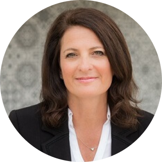
Jackie Mattox
Founder,
President and CEO
Women in Electronics

Ashley Quinlan
VP of Global Distribution and
Marketing Strategy

Chris Church
Co-founder
Chief Product Officer
Macrofab

Leigh Gawne
Chief Technology Officer
Altium

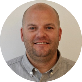
Dave Doherty
President and COO
Digi-Key Electronics

Robert Feranec
Founder & CEO
FEDEVEL Academy
Dan Schoenfelder
Head of Octopart
Octopart/Nexar
Agenda Highlights
Learn from the top experts across the industry about the most cost-effective and easy way to manufacture your boards in the age of connectivity.
- Design Principles & Practices
- Simulation, Test, & Measurement
- Supply Chain
- Manufacturing
Frequently Asked Questions
Learn, connect and get inspired at this 3-day event featuring live workshops, professional development courses and exciting industry keynote to help you achieve success through every stage of the PCB Design Process, from conception to the finished product.
At Altium we believe education, networking and professional development should be accessible to everyone, whether you are a professional, student or self-starter.
The virtual event experience will be available 24 hours before the first dayfirst keynote. In this timeframe you can get accustomed to the platform, set up your profile, visit exhibitors and start networking.
The full agenda will be made available five weeks prior to the event
The virtual experience is optimized for the Google Chrome Browser. Expect issues with the stream if you are joining from an office environment with strict firewall and access restrictions. A broadband internet connection is recommended.
To win the prize you need to reach the top of the leaderboard by being an active user on the platform. You will be able to see the point distribution next to the leaderboard. The more you participate in the event on our platform, the more likely you are to win. For more detailed rules and requirements to participate click here
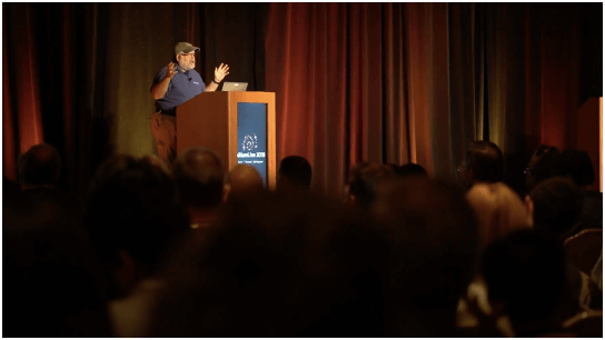
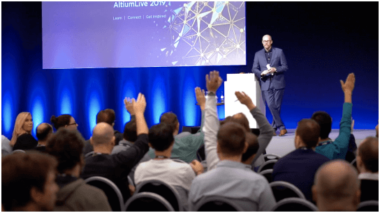
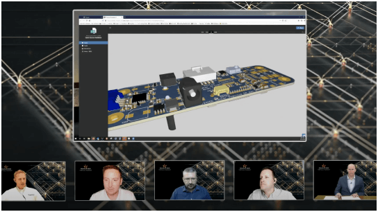
Retrospective
Explore AltiumLive's History in Video
- 2017
- 2018
- 2019
- 2020