
Создание посадочного места
The real-world component that gets mounted on the board is represented as a schematic symbol during design capture, and as a PCB footprint for board design. Altium Designer components can be:
- Created in and placed from local libraries or
- Placed directly from a managed content server – a globally accessible component storage system that contains thousands of components, each with a symbol, footprint, component parameters, and links to suppliers.
Manually Creating a Footprint
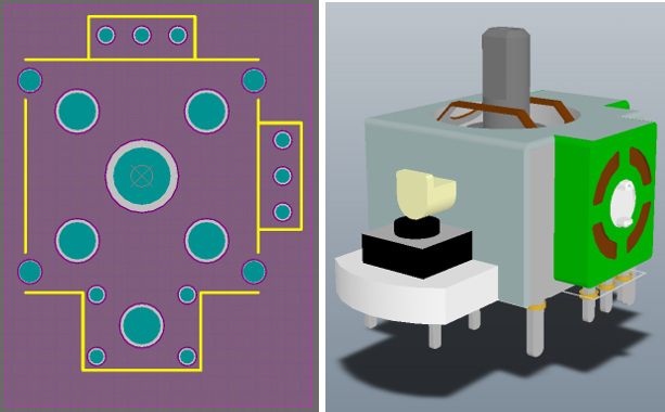 2D and 3D views of a footprint for a joystick component. The 3D image shows the imported STEP model for the component. Note
the pads and component overlay can be seen below the STEP model.
The typical sequence for manually creating a component footprint is:
- Footprints should be built around the workspace reference point at the center of the PCBLIB editor. Use the J, R shortcut keys to jump directly to the reference point. If you have forgotten to move to the reference point before beginning to build your footprint, you can bring the reference pad to your footprint using the Edit » Set Reference sub-menu commands.
- Place the pads (Place » Pad) according to the component requirements. After running the place Pad command but prior to placing the first pad, press the Tab key to open the Properties panel to define all the pad properties, including the pad Designator, Size and Shape, Layer, and Hole Size (for a thru-hole pad). The Designator automatically increments for subsequent pad placements. For a surface mount pad, set the Layer to Top Layer. For a thru-hole pad, set the Layer to Multi-Layer.
- To ensure accurate placement of the pads, consider setting up a grid specifically for the task. Use the Ctrl+G shortcut keys to open the Grid Editor dialog and the Q key to toggle the grid from Imperial to Metric.
- To accurately place a pad while moving it with the mouse, use the keyboard arrow keys to move the cursor in current grid increments. Additionally, holding Shift will move in steps of 10 times the grid. The current X, Y location is displayed on the Status bar and also in the Heads Up display. The Heads Up display contains both the location and the delta from the last click location to the current cursor location. Use the Shift+H shortcut to toggle the Heads Up display on and off. Alternatively, double-click to edit a placed pad and enter the required X and Y locations in the Properties panel.
- To check a distance between two points in the workspace, use the Reports » Measure Distance (shortcut Ctrl+M). Follow the prompts on the Status bar.
- Pad-specific attributes, such as solder mask and paste mask, are automatically calculated based on the pad dimensions and applicable mask design rules. While mask settings can be defined manually for each pad, doing so makes it difficult to modify these settings later during the board design process. Typically this is done only when it is not possible to target the pads by design rules. Note that rules are defined in the PCB editor during board design.
- Use tracks, arcs and other primitive objects to define the component outline on the silkscreen layer.
- Place tracks and other primitive objects on a mechanical layer to define extra mechanical detail, such as a placement courtyard. Mechanical layers are general-purpose layers. You should allocate the function of these layers and use them consistently across their footprints.
- Place 3D Body objects to define the three-dimensional shape of the component that fits on the footprint. Multiple 3D Body objects can be placed to build up the shape, or a STEP format 3D component model can be imported into a 3D Body object.
- The Designator and Comment strings are automatically added to the footprint’s Overlay layer during placement into the main PCB workspace. Additional Designator and Comment strings can be included by placing the
.Designatorand.Commentspecial strings on a mechanical layer. - Rename the completed footprint by double-clicking on its name in the Footprints list in the PCB Library panel to open the PCB Library Footprint dialog. Enter the desired name; names can be up to 255 characters.
Creating a Component using the IPC Compliant Footprint Wizard
The IPC Compliant Footprint Wizard creates IPC-compliant component footprints. Rather than working directly from footprint dimensions), the IPC Compliant Footprint Wizard uses dimensional information from the component itself then calculates suitable pad and other footprint properties in accordance with the algorithms released by the IPC.
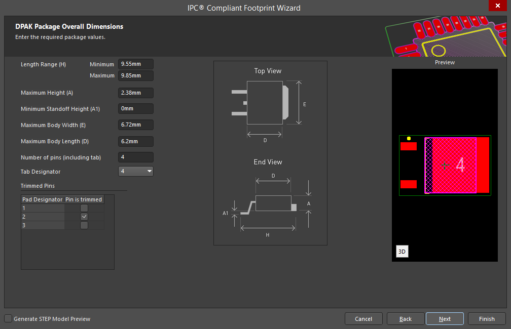
One of the supported packages in the IPC Compliant Footprint Wizard is the DPAK (Transistor Outline).
- Select Tools » IPC Compliant Footprint Wizard to run the IPC Compliant Footprint Wizard.
- The wizard can create the following footprint type: BGA, BQFP, CAPAE, CFP, CHIP Array, DFN , CHIP, CQFP, DPAK, LCC, LGA, MELF, MOLDED, PLCC, PQFN, PQFP, PSON, QFN, QFN-2ROW, SODFL, SOIC, SOJ, SON, SOP/TSOP, SOT143/343, SOT223, SOT23, SOT89, SOTFL, and WIRE WOUND.
- The IPC Compliant Footprint Wizard uses dimensional information from the component itself in accordance with the standards released by the IPC.
Some of the IPC Compliant Footprint Wizard features include:
- Overall packaging dimensions, pin information, heel spacing, solder fillets, and tolerances can be entered and immediately viewed.
- Mechanical dimensions, such as Courtyard, Assembly, and Component (3D) Body Information, can be entered.
- The Wizard is re-entrant and allows reviewing and making adjustments easy. Previews of the footprint are shown at every stage.
- The finish button can be pressed at any stage to generate the currently previewed footprint.
Creating a Component Using the IPC Footprint Batch Generator
The IPC Footprint Batch Generator can be used to generate multiple footprints at multiple density levels. The generator reads the dimensional data of electronic components from an Excel spreadsheet or comma delimited file then applies the IPC equations to build IPC compliant footprints. Support for the IPC Footprints Batch Generator includes:
- Package type blank template files are included in the
\Templatesfolder in the Altium Designer installation. - Package input files can contain the information for one or more footprints of a single package type and can be either an Excel or comma-delimited (CSV) format file.
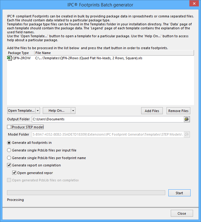
The IPC Footprints Batch Generator has options to either create all the footprints in the open PCB footprint
library or generate a single library based on either an input file or footprint name.
Creating a Component using the Footprint Wizard
The PCB Library Editor includes a PCB Component Wizard. This Wizard allows you to select from various package types and fill in appropriate information and it will then build the component footprint for you. Note that in the PCB Component Wizard you enter the sizes required for the pads and component overlay.
To launch the PCB Component Wizard, right-click on the Footprints section of the PCB Library panel then select Footprint Wizard or select the Tools » Footprint Wizard command from the main menus.
Including a 3D Model of the Component
A 3D representation of the component can be included in the footprint. The following 3D model formats can be used in Altium Designer:
- Altium Designer 3D Body Objects - place these to build up the required component shape.
- STEP models -
*.Stpand*.Step. - SolidWorks parts -
*.SldPrt. - Parasolid Models -
*.x_tand*.x_b.
The shape can be created by placing a number of Altium Designer 3D Body objects to build up the shape by placing one 3D Body object and importing a 3D model into it or a combination of both.
- Allocate a mechanical layer for 3D Body objects then during placement, ensure that this layer is selected in the Properties panel.
- Building a component shape from 3D Body objects is generally easier with the display in 2D mode. Available shapes for 3D Body objects include extruded, cylindrical or spherical.
- To switch the PCB Library editor between 2D and 3D display modes, press the 2 and 3 hotkey shortcuts.
- 3D component models can be downloaded from component manufacturer websites or shared resource sites such as www.3dContentCentral.com.
- 3D models are easier to place with the display in 3D mode. To place a Generic 3D model, first place a 3D Body object, when the Properties panel opens, set the 3D Model Type to Generic, select the Embed Model option in the Source region. Click the Choose button to browse and locate the 3D model file.
- When a 3D model is clicked and held to be moved, it will be held by the nearest vertex belonging to the 3D Body object the 3D model is embedded in or by a snap point defined on the 3D model. Snap Points can be defined in the Properties panel Snap Points region or by using the Tools » 3D Body Placement » Add Snap Points From Vertices command. This command is interactive; watch the Status bar for prompts. Note that the command has two modes. The default is to add a Snap Point at the vertex chosen by the user. The second mode is enabled by pressing the Spacebar after launching the command. In this mode the Status bar prompts you to click on two points. The software then calculates and positions the Snap Point at the mid-point of the two clicks.
- Use the standard Windows shortcuts to zoom and pan when the PCB Library editor is in 3D display mode. As in 2D mode, click and hold the right-mouse button to pan or slide the document. To rotate the view, hold the Shift key then click and hold the right-mouse button. Alternatively, use a 3D mouse, such as the Space Navigator™.
- The List panel is good for editing 3D Body object properties, such as dimension, rotation and color. These panels allow you to easily edit a value and immediately see the impact – ideal for tasks such as rotating a 3D model.
- 3D model support is not limited to components. It also can be used to import other mechanical detail such as a bracket or the finished enclosure. Import the enclosure directly into the PCB editor. If it is linked rather than embedded, when a change is made to the linked 3D model, a warning dialog pops up in the PCB editor offering to reload the 3D model.

The same footprint: on the left, the physical component has been created from a set of 3D Body objects; on the right, a STEP model has been imported.
Creating Footprints with Irregular Shapes
Some footprints require pads that have an irregular shape. This can be done using any of the design objects available in the PCB Library Editor, but when doing this, there is an important factor that must be kept in mind.
Create irregular shaped pads by placing multiple objects.
Altium Designer automatically adds solder and paste masks to pad objects based on their shape. Default expansion values are defined by design rules by default, although they can also be specified by the Pad settings contained on the PCB Editor - Defaults page of the Preferences dialog. These settings can be overridden during placement or after placement through the Properties panel.
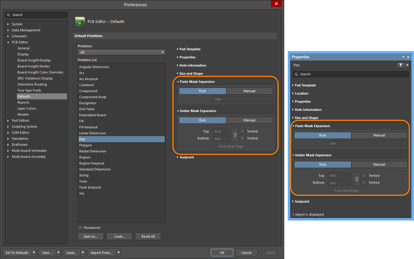
Creating a Custom Pad Shape
Main article: Working with Custom Pad Shapes
If only pad objects have been used to build up an irregular shape, the matching irregular mask shape will automatically be generated as an expansion of the pad shape. But if the irregular shape was built up using other objects, such as lines (tracks), fills, regions, pads, vias, or arcs, the solder and paste masks will need to be configured manually.
All object-kinds have a solder mask property, and fill and region objects also have a paste mask expansion property. If these objects have been placed on the top layer to create a pad shape, then the solder mask property of those objects can be enabled to either obey the applicable design rule, or use a manual expansion value. If fill and region objects have been used to build up a pad shape, then the paste mask can also be enabled as a property of the extra objects.
When the mask shape is not correctly created as an expansion (or contraction) of the set of objects used to create the custom pad shape, then manually defined solder and paste mask expansions can be also achieved by placing lines (tracks), fills, regions, or arc primitives directly on the corresponding solder or paste mask layer. The custom button footprint shown below is an example of this.
Displaying Solder / Paste Masks
To check that solder and/or paste masks have been correctly defined in the PCB Library Editor, open the View Configuration panel and enable the show option ( ![]() ) option for each mask layer.
) option for each mask layer.
The image in the Footprints with Multiple Pads Connected to the Same Pin section below shows a PCB footprint with a purple (color of the Top Solder Mask layer) border that appears around the edge of each pad. This represents the edge of the solder mask shape protruding by the expansion amount from under the pad.
To quickly walk through layers, use the Single Layer Mode (Shift+S) in combination with Ctrl+Shift+Wheel roll.
Managing Components with Routing Primitives
When a design is transferred, the footprint specified in each component is extracted from the available libraries and placed on the board. Then each pad in the footprint has its net property set to the name of the net connected to that component pin in the schematic. All objects touching a pad connect to the same net as the pad.
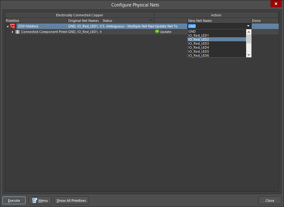
The PCB Editor includes a comprehensive net management tool. To launch it select Design » Netlist » Configure Physical Nets from the main menus to open the Configure Physical Nets dialog. Click the Menu button for a menu of options. Click the New Net Name header drop-down to select the net to assign to the unassigned primitives.
Footprints with Multiple Pads Connected to the Same Pin
The footprint shown below, a SOT223 transistor, has multiple pads that are connected to the same logical schematic component pin - Pin 2. To make this connection, two pads have been added with the same designator - '2.' When the Design » Update PCB command is used in the Schematic Editor to transfer design information to the PCB, the resulting synchronization will show the connection lines going to both pads in the PCB Editor.
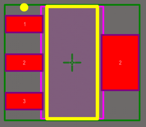
SOT223 footprint showing two pads with a designator of 2.
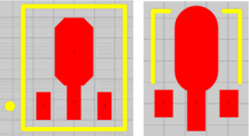
Handling Special Solder Mask Requirements
The footprint shown below is the contact set for a push button switch implemented directly in the copper on the surface layer of the PCB.
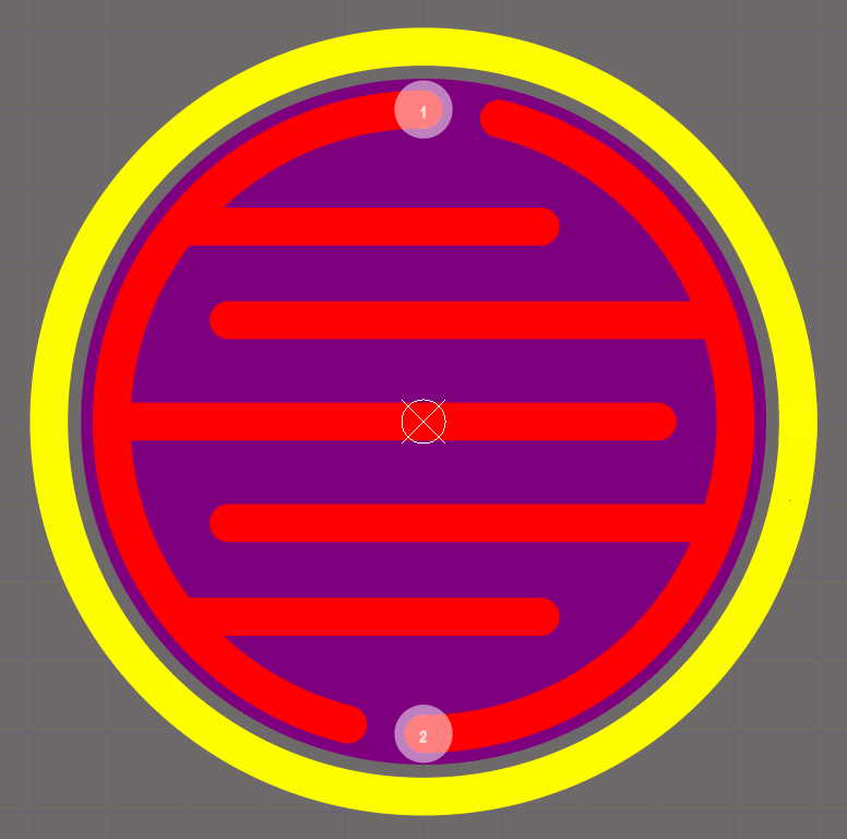
Printed push button footprint designed by placing pads, lines and arcs.
A rubber switchpad overlay is placed on the PCB, with a small captive carbon button that contacts both sets of fingers in the footprint when the button is pressed to create the electrical connectivity. For this to happen, both sets of fingers must not be covered by the solder mask.
The circular solder mask opening has been achieved by placing an arc whose width is equal to or greater than the arc radius, resulting in the solid purple circle shown behind the two sets of fingers. Each set of copper fingers has been defined by an arc, horizontal lines, and a pad (selected in the image to make them visible). The pads are required to define the points of connectivity. Manually placed top solder mask definitions are automatically be transferred to the bottom side solder mask layer if the component is placed on the bottom side of the board.
Designator and Comment Strings
Default Designator and Comment Strings
When a footprint is placed on a board, it is given a Designator and Comment based on information extracted from the schematic view of the design. Placeholders for the Designator and Comment strings do not need to be manually defined since they are added automatically when the footprint is placed on a board. The locations of these strings is determined by the Designator and Comment string Autoposition option in the Properties panel. The default position and size of Designator and Comment strings is configured in the respective Primitive on the PCB Editor - Defaults page of the Preferences dialog.
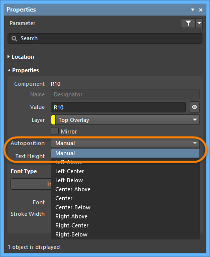
Additional Designator and Comment Strings
There may be situations where additional copies of the Designator or Comment strings are required. For example. the assembly house might want a detailed assembly drawing with the designator shown within each component outline, while in-house company requirements stipulate the designator to be located just above the component on the component overlay on the final PCB. This requirement for an additional designator can be achieved by including the .Designator special string in the footprint. A .Comment special string also is available for stipulating the location of the comment string on alternate layers or locations.
To cater for the assembly house's requirements, the .Designator string would be placed on a mechanical layer in the library editor and print outs that included this layer could then be generated as part of the design assembly instructions.
Handling Special Layer-specific Requirements
There are a number of special requirements a PCB component can have, such as needing a glue dot or a peelable solder mask definition. Many of these special requirements will be tied to the side of the board on which the component is mounted and must flip to the other side of the board when the component is flipped.
Rather than including a large number of special purpose layers that may rarely be used, Altium Designer's PCB editor supports this requirement through a feature called layer pairs. A layer pair is two mechanical layers that have been defined as a pair. Whenever a component is flipped from one side of the board to the other, any objects on a paired mechanical layer are flipped to the other mechanical layer in that pair.
The Names of Mechanical Layers can be edited directly from the View Configurations dialog by right-clicking then selecting Edit Layer.
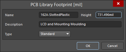
Adding Height to a PCB Footprint
At the simplest level of 3D representation, height information can be added to a PCB Component. To do this, double-click on a footprint in the Footprints list in the PCB Library panel to open the PCB Library Footprint dialog. Enter the recommended height for the component in the Height field.
Height design rules can be defined during board design (click Design » Rules in the PCB Editor), typically testing for maximum component height in a class of components or within a room definition.
A better option for defining height information would be to attach 3D Bodies and/or a STEP model to the PCB Component. Details of this will be discussed in another module.
Adding Footprints from Other Sources
PCB Components can be copied from other PCB Libraries and then renamed and modified within the destination library to match the specifications required. There are a number of ways to execute this function.
- Select placed footprint(s) in a PCB document then copy (Edit » Copy) and paste them into an open PCB library using Edit » Paste Component.
- Select Edit » Copy Component when the footprint to be copied is active in the PCB Library Editor, change to the open PCB destination library then select Edit » Paste Component.
- Select one or more footprints in the list in the panel using the standard Shift+Click or Ctrl+Click, right-click then choose Copy. Switch to the target library, right-click in the list of footprint names then choose Paste.
Validating Component Footprints
There are a series of reports that you can run to check that footprints have been created correctly as well as identifying which components are in the current PCB library.
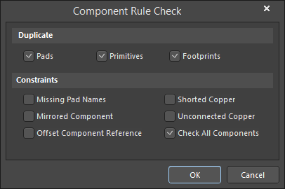
The Component Rule Check report (Reports » Component Rule Check) is useful for validating all components in the current PCB library by testing for duplicate primitives, missing pad designators, floating copper, and inappropriate component references.
Validating PCB Libraries within an Integrated Library
Including PCB Libraries as part of a Integrated Library Package provides an additional layer of validation because it allows the Design Compiler to examine the Schematic and PCB models together. This, of course, requires that a Schematic Library that matches the PCB Library exists however assuming this is the case, a range of additional checks are possible using the Error Reporting tab of the Project Options dialog.
Updating a PCB Footprint
Updating a PCB Footprint can be done in two ways: "Pushing" the PCB from the PCB Library, or by "Pulling: from the PCB Editor. Pushing a PCB Footprint update takes a selected footprint(s) from the PCB Library and uses it to update all open PCB documents containing that footprint. This first method is the best option when a complete replacement is desired. The second option allows you to review all the differences between the existing footprint and the footprint in the library before the update is performed. You can also select which objects are to be updated from the library. This second method is the best option when you need to figure out exactly what has changed between the footprint on the board and the footprint in the library.
Pushing Footprint Updates from the PCB Library
From the PCBLIB Editor, use the Tools » Update PCB with Current Footprint or Tools » Update PCB With All Footprints command. From the PCB Library panel, right-click in the Components region of the PCB Library panel then select Update PCB with [Component] or Update PCB with All. Running these commands opens the Component(s) Update Options dialog from which you can select the primitives/attributes to be updated.
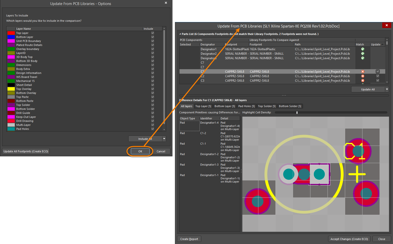
Pulling Footprint Updates from the PCB Editor
From the PCB editor, use the Tools » Update From PCB Libraries command, which, in turn, opens the Update From PCB Libraries - Options. Click OK to open the Update From PCB Libraries dialog.
Releasing Completed PCB Footprints to a Server
After completing the creation of a PCB Footprint, the footprint and any additional 3D model/body information (all of which comes together to create the component model) can be released to and stored in a server. A server-based component gathers together all information needed to represent that component across all design domains within a single entity. It could, therefore, be thought of as a container in this respect. A 'bucket' into which all domain models and parametric information is stored.
In terms of its representation in the various domains, a server-based component does not contain the domain models themselves, but rather links to these models. These links are specified on the design side, as part of the source component definition from which the released Component Item is generated. As such, before you can delve into the process of defining and releasing server-based components, you must first ensure that all the domain models themselves have been created and released.