Working with the Power Plane Clearance Design Rule on a PCB in Altium Designer
Created: марта 23, 2017 | Updated: января 06, 2021
| Applies to versions: 18.0, 18.1, 19.0, 19.1, 20.0, 20.1 and 20.2
Вы просматриваете версию 18.1. Для самой новой информации, перейдите на страницу Working with the Power Plane Clearance Design Rule on a PCB in Altium Designer для версии 21
Rule category: Plane
Rule classification: Unary
Summary
This rule specifies the radial clearance created around vias and pads that pass through but are not connected to a power plane.
Constraints
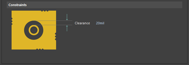
 Default constraints for the Power Plane Clearance Rule.
- Clearance - the value for the radial clearance.
How Duplicate Rule Contentions are Resolved
All rules are resolved by the priority setting. The system goes through the rules from highest to lowest priority and picks the first one whose scope expression matches the object(s) being checked.
Rule Application
During output generation.
