
Аннотирование компонентов
Design Annotation is the systematic and methodical process for ensuring that each component in the design can be individually identified by means of a unique designator. While Altium NEXUS is able to maintain the identity of components using Globally Unique IDs (GUIDs), most designers historically use the component's designator as the primary means of referencing the component across the schematic (logical) and PCB (physical) domains, as well as in outputs such as the Bill of Materials (BOM).
There are three approaches to annotating a design. The choice of Annotation tool depends on a number of factors including the type of design, personal preference, and company policy and procedures.
Schematic Level Annotation
Schematic Level Annotation uses a purely logical view of the design to determine component designators. It is most useful for simple designs that do not use Device Sheets, but because it allows the order of processing to be specified as well as the option to complete existing packages for multi-part components, it is also a pre-requisite to Board Level Annotation.
In summary, use Schematic Level Annotation to:
- Package multi-part components.
- Annotate components based on their position in the schematic design.
- Annotate multi-channel designs using the default naming scheme as specified in the Project Options.
- Prepare a design for additional annotation.
PCB Annotation
PCB Annotation uses the physical location of components on the PCB to determine their designation. This allows positional information to be effectively encoded into a component's designator and can be very helpful when debugging an assembled PCB. In short, you should use PCB Annotation to annotate components based on their position on the board in the PCB Design.
Board Level Annotation
Board Level Annotation provides a mapping between designators used in the schematic (logical) design and their real-world counterparts on the PCB (physical) design. While Board Level Annotation can be used in any design, it is especially useful for multi-channel designs or designs that incorporate device sheets where the designators cannot be edited on the device sheet itself. In this way, the entire design can be re-annotated without actually modifying the original device sheet(s). Board Level Annotation resolves any conflicting annotation problems that may occur due to duplicate designators across a project and stores its changes in an *.Annotation text file. It includes additional keywords for customizing naming schemes and allows them to be applied to all or only a select range of parts.
In summary, use Board Level Annotation to:
- Annotate the compiled components in device sheets.
- Uniquely name all components across several channels using naming schemes, which include positional annotation, global indexing, and other configurable options.
- Manually name components.
Schematic Annotation
The Annotate Schematics command systematically assigns designators to all or selected parts in selected sheets of a project and ensures that designators are unique and ordered based on their position. Annotation options can be configured to package multi-part components, set index and suffix options, reset schematic designators including any duplicate designators, and back annotate from the PCB.
The Annotate Schematics command is accessible from the menu by clicking Tools » Annotation » Annotate Schematics.

The Annotate dialog is launched from the Annotate Schematics command.
The Annotate dialog is divided into two primary regions:
- The left side is for configuring the Order of Processing, setting Matching Options for multi-part components, determining the process location of the desired designator or part, and setting the scope of annotation, including setting an index and adding a suffix for designators per schematic sheet.
- The right side lists the proposed changes that will occur once the Accept Changes (Create ECO) button is clicked. It includes the Current and Proposed designators along with the option to lock (exclude) specific designators and/or sub-parts from annotation.
Order of Processing
Positional annotation is directed through the Order of Processing option. The four options shown below are available to control how schematic documents will be scanned.

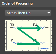
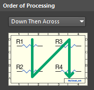
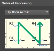
Specify the order that components will be processed.
Matching Options

Matching components into multi-part packages.
When using multi-part packages, it is often desirable to pack as many parts into the minimum number of physical parts since this minimizes the overall BOM cost of the design. Primary considerations for annotating multi-part components are how those components will be matched and grouped together and the criteria used to determine valid groupings.
Complete Existing Packages
In order for multi-part packing to be included as part of the annotation process, the Complete Existing Packages drop-down must be set to something other than None.
- None - existing packages will not be completed and all new parts will be placed into new packages.
- Per Sheet - existing packages will include only new parts from the same schematic sheet.
- Whole Project - existing packages will include new parts from any of the schematic sheets in your project.
Lock Components
For non-homogeneous multi-part components, ensure the Locked icons are closed in the Properties panel to prevent sub-part changes during annotation.
Component Parameters
The Component Parameter list includes all parameters found within components in the current design. If multi-part components share the same enabled parameters and a common value, then they will be packaged together (assuming the Complete Existing Packages option is not set to None).
The default settings in the Annotate dialog are to complete existing packages by Library Reference and Comment, however, you can select any combination of parameters.
Strictly Option
If the Strictly checkbox is enabled for a Component Parameter, all components must have that parameter matched into a package. Components that do not have this parameter are annotated as individual components and are not packaged.
The following example illustrates how these options combine to give a specific result:
Consider a design with eight OR Gates and eight resistors (as shown in the image below). The OR gates contain a parameter called QuadOrGate, with one group of four OR gates having the parameter value Package1 and the other group of four OR Gates having the parameter value Package2. The resistors have no such parameter. Enabling the checkbox for QuadOrGate in the Component Parameter control will ensure that this parameter is used to control how components are packaged; in this case, the Strictly check box is not enabled.
After launching the Tools » Annotation » Annotate Schematics command, parts with the parameter QuadOrGate = Package1 will be packaged into the same physical component and those that have the parameter QuadOrGate = Package2 will be packaged together separately. Any remaining components that do not have the QuadOrGate parameter will be packaged together. In this case, the resistors are packaged together since their common attribute is that they do not contain the QuadOrGate parameter.

Example of packaged components when the Strictly option is unchecked.
If the same design is annotated but the Strictly option is checked, only those components that have the QuadOrGate parameter will be packed. In this case, the OR gates will be packed but the resistors will be left unpacked. Consequently, while the Strictly option provides extremely fine control over the packing process, most situations will call for it to be unchecked.
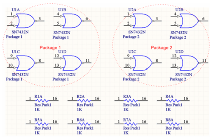
Example of packaged components when the Strictly option is checked.
Schematic Sheets to Annotate
A high degree of control is provided over which schematic sheets and components will be affected by annotation and the specifics of how those changes will be calculated.

Specifying the scope of annotation.
- A check in the box to the left of the listed schematic sheet indicates that it will be processed as part of the annotation command.
- The scope of annotation is determined by the Annotation Scope drop-down list and can be expanded to include the entire schematic sheet or limited to (un)selected components. Using the Ignore Selected Parts or Only Selected Parts options requires that the components were selected in the design prior to running the Annotation command.
- Configure the order in which the schematic sheets are to be annotated using the Order field. Type a value directly into the field or use the arrows that appear once you click in the field to set the desired value.
- If the Designator Index Control option is checked, the designator value will begin from the Start Index value. The Start Index has no effect if the Designator Index Control option is not checked.
- An additional suffix can be added to the end of each designator by specifying a string/value in the associated Suffix column. Avoid using single character suffixes such as 'A' or '1' as these can be easily confused with sub-parts and/or other designator values.
Proposed Change List
Click the Update Changes List button to update the Proposed Change List so that all designator changes can be reviewed prior to being applied. Only designators that have not previously been set (i.e. R?, C?, etc.) will be affected by the changes. Therefore, if the intention is to update all designators in the design, they should first be reset by pressing the Reset All button.

Resetting designators prior to applying the annotation settings.
The Proposed Change List lists all designators for the parts contained within the sheets selected for annotation. For each entry, details of the Current and Proposed Designator values are included along with the component's Sub (part) and the source Location of Part.
Checking the box associated with a Designator will lock that specific designator from any changes. Similarly, checking the Sub box will prevent that specific multi-part component from being updated. This option can be used as an alternative to setting the Lock icon in the Properties panel.
After reviewing the list of proposed changes, click the Accept Changes (Create ECO) button to launch the Engineering Change Order dialog. Once the ECO is executed, the annotation changes will be applied to the design.
Additional Schematic Annotation Commands
The Tools » Annotation menu contains a number of targeted Schematic Annotation commands. The first item in the group, Annotate Schematic, has already been discussed.

Various available annotation commands
Reset Schematic Designators
If large portions of content have been cut and pasted from different sources into a new design, it may be necessary to reset all designators. Because this command uses settings taken from the Annotate dialog, it will be applied to items previously set within that dialog. For instance, if all Schematic Sheets To Annotate were previously checked, then the Reset Schematic Designators command will apply to the entire project whether the sheets are currently opened in the editor or not. If only a few Schematic Sheets To Annotate were previously checked, then the Reset Schematic Designators command will only affect those sheets.
Any designators with a locked status are not reset or changed in any way.
Reset Duplicate Schematic Designators
When duplicating portions of a design, the newly-copied components will still hold the same designator values as those from which they were copied. The Reset Duplicate Schematic Designators command provides a fast way to reset duplicate designators to '?'. Because this command uses settings taken from the Annotate dialog, it will be applied to items previously set within that dialog. For instance, if all Schematic Sheets To Annotate were previously checked, then the Reset Duplicate Schematic Designators command will apply to the entire project whether the sheets are currently opened in the editor or not. If only a few Schematic Sheets to Annotate were previously checked, then the Reset Schematic Designators command will only affect those sheets.
Any designators with a locked status are not reset or changed in any way.
Annotate Schematics Quietly
The Annotate Schematics Quietly command makes it possible to apply all of the previous settings of the Annotate dialog without needing to reopen the main dialog.
Force Annotate All Schematics
Running the Force Annotate All Schematics command is equivalent to running the Reset Schematic Designators command followed immediately by the Annotate Schematics Quietly command. Consequently, the Force Annotate All Schematics command uses settings that were previously set within the Annotate dialog when determining which components and sheets can be updated.
After launching this command, a request for confirmation appears that details the number of designators that will be updated if accepted.
Back Annotate Schematics
Prior to the introduction of Altium NEXUS's Design Compiler and Synchronizer, annotation changes were historically passed from the schematic to the PCB via a netlist (*.net) file. Annotation changes that needed to propagate in the reverse direction - from the PCB to the schematic - were handled via a Back Annotation process. This process uses a Was-Is (*.WAS) file or Engineering Change Order (*.ECO) file to direct the changes to be applied to schematic designators.
Number Schematic Sheets
The Number Schematic Sheets command does not alter component designators but rather schematic sheet designators (numbers). Conceptually, it is therefore related to the general concept of design annotation.
Sheet and document numbering allows you to take control over the sheet designation and store them as parameters within the respective schematic documents. Altium NEXUS's special string feature (=SheetNumber, =DocumentNumber, =SheetTotal) can then be used to expose these values on the sheet (in the sheet footer, for example) as text objects.

Numbering schematic sheets.
The process of numbering sheets is as follows:
Automatic Sheet Numbering (Project Option)
Enable to perform automatic sheet numbering. The values will be displayed in the Projects panel. You can also enable automatic sheet numbering by checking the Automatic Sheet Numbering option on the Options tab of the Project Options dialog.
Auto Sheet Number
Click on the Auto Sheet Number drop-down button to access the sheet numbering options.
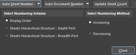
The Select Numbering Scheme options are:
- Display Order - the sheets are numbered in the order they are displayed.
- Sheets Hierarchical Structure - Depth First - the sheets are numbered from the top level into each branch. The top-level is numbered first then the first branch under the top level is numbered completely, the second branch, and so on.
- Sheets Hierarchical Structure - Breadth First - the sheets are numbered according to their level in the hierarchy. The top-level is numbered first, all second levels are numbered next, and so on.
The Select Numbering Method options allow for Increasing or Decreasing sequential values to be selected.
Auto Document Number
Click on the Auto Document Number drop-down to access the document numbering options. They are essentially the same as the Auto Sheet Number options except with the addition of Prefix and Postfix values.
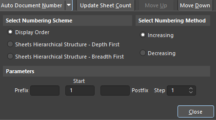
The Parameters options are as follows:
- Prefix - choose a prefix to place in front of your document number. Alpha (
A,B,C, etc.,), numeric, (1,2,3, etc.,) and non-numeric (_,*,.,%, etc.,) prefixes are supported including combinations of all of them. - Start - choose a numerical value from which to begin numbering.
- Postfix - choose a postfix to append to the document number. Alpha (
A,B,C, etc.,), numeric (1,2,3, etc.,) and non-numeric (_,*,.,%, etc.,) postfixes are supported including combinations of all of them. - Step - choose a value to increment each document number by. For example, if the Start index is set to 1 and the Step value is set to 100, the first document number will be 1 and the next document number will be 101 (Start + Step), the next 201, and so on.
Update Sheet Count
Click on the Update Sheet Count button to tally up the number of sheets in the current project and place the result in the SheetTotal column. The sheet count will be the total number of sheets in the project regardless of the numbering scheme selected in either of the previous controls.
Move Up/Down
Use the Move Up or Move Down buttons to move a selected schematic document up or down in the list. This is relevant when using the Display Order numbering scheme to specify Sheet or Document Numbers.
Custom Numbering/Naming
If an organization has a specific number or naming system that cannot be automated through either the Auto Sheet Number or Auto Document Number commands, custom sheet names and numbers can be written directly into the SheetNumber or DocumentNumber fields.
Schematic Sheet Numbering and Device Sheets
Sheet or Document Numbers cannot be configured for Device Sheets when they are read-only (default state) and will be cross-hatched in the Sheet Numbering For Project dialog to indicate they cannot be updated. When Device Sheets are set as editable, the cross-hatching is removed and Sheet and Document Numbering can be configured as normal.
Board Level Annotation
Board Level Annotation is the process of annotating the compiled components (the physical view of your components) of your design through the Schematic Editor. Board Level Annotation allows you to either name your components based on a number of naming schemes or specify custom names.
Board Level Annotation gives you complete control over the annotation in your project with annotation settings saved in an *.Annotation text file displayed under the Settings\Annotation Documents sub-folder in the Projects panel. Altium NEXUS manages Annotation files automatically.
You can choose to name all of the components in your project, name selected components, or name only those components that are not designated. To annotate the compiled components in your project through the Schematic Editor:
- Ensure that the components have been annotated at the schematic level so that the schematic source data, including packaged options for multi-part components, is available as input for your Board Level Annotation.
- Select Tools » Annotation » Board Level Annotate (shortcut Ctrl+L) which brings up the Board Level Annotate dialog. The left side of the dialog is for filtering and setting the scope of annotation; the right side shows the proposed changes.

The Board Level Annotate dialog displays all of the schematic documents in your project.
Filter Options
The left side allows you to control the scope of annotation at the Sheet, Channel and Part Level. The columns in the Filter Options region do not change.
Schematic Sheet
The Schematic Sheet column lists all of the schematic documents in your project. A schematic document may be listed more than once if your design includes multiple channels.
Channel Name
The Channel Name column lists all of the relevant channels in your design. If there are no channels in the design, this column will be populated with the schematic sheet name.
Enabled
Check this box to include the associated Schematic Sheet for a specific Channel in this Board Level Annotation. Uncheck the box to exclude this sheet from Board Level Annotation.
Annotation Scope
Choose from the following to set the scope for the parts to be annotated:
- All - all parts in the Schematic Sheet will be annotated.
- Ignore Selected Parts - all parts except those selected will be annotated.
- Only Selected Parts - only the parts selected will be annotated.
All On, All Off Buttons
When pressed, the All On button checks the Enabled checkbox for all schematic sheets in the project. The All Off button disables the Enabled checkbox for all schematic sheets in the project.
Proposed Change List
The right side of the dialog allows you to view Schematic Source Components, view Calculated Design Data used in the current naming scheme whether this is the default name for compiled components or the applied naming scheme, (highlighted in green), apply a Naming Scheme and view the resultant PCB Component Instance.
Schematic Source Component
The Schematic Source Component section is made up of three columns:
- Hierarchy Path - the path of the schematic source in the format Filename\Channel.
- Prefix - the alphabetical prefix extracted from the Schematic Level Designator. For example, if your Schematic Level Designator is
R13, the Prefix isR.
 denoting that the component has a designator. If you reset the designators, the icon will revert to
 - Local Index - the index you have specified following the alphabetical prefix extracted from the schematic level designator. For example, if the schematic level designator is
R13, the Local Index is13.
Calculated Design Data
Upon first opening the Board Level Annotate dialog, the Calculated Design Data section displays the Room name column, which corresponds to the default Annotate Option selected. Once you have performed a Board Level Annotation, the columns displayed in the Calculated Design Data represent the keywords selected in your naming scheme for annotation in your Annotate Options. These columns are updated dynamically based on your selection. For example, if you select your Naming Scheme to be $GlobalIndex.$SheetDesignator, the columns displayed will be Global Index and Sheet Designator.
Naming Scheme
Check the box to enable the Naming Scheme for this component; uncheck the box to disable. Note that when this field is unchecked, the PCB Component Instance column can be edited so you can specify a custom designator for your component.
PCB Component Instance
The PCB Component Instance column displays the proposed designator. This field is dictated by either the Naming Scheme selected or a custom value that can only be specified when the Naming Scheme field is unchecked. The custom name can contain any combination of alphanumeric and non-alphanumeric characters.
Annotate Options
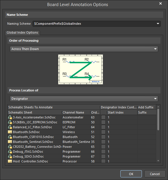
Annotate Options (accessed by clicking the Annotate Options button in the Board Level Annotate dialog) allows you to further customize your Annotation using either predefined or custom Naming Schemes.
Predefined Naming Schemes
To apply a predefined naming scheme:
- From the Board Level Annotate dialog, click the Annotate Options button to open the Board Level Annotation Options dialog.
- Select a predefined Naming Scheme from the drop-down list.
- Once you have selected a naming scheme, customize any other options such as Global Index Options or Room Name Options, click OK. Customization options vary between predefined naming schemes.
- Notice that the Calculated Design Data columns are updated to reflect the keywords used in your Naming Scheme.
Custom Naming Schemes
To apply a custom naming scheme:
- From the Board Level Annotate dialog, click the Annotate Options button to open the Board Level Annotation Options dialog.
- Define your own Naming Scheme using valid keywords by typing directly into the Naming Schemes field. You can select any combination of valid keywords in any order to define your own naming scheme. You can use any non-alphanumeric character in your Naming Scheme to separate keywords, for example, "_", "*", ".", and "@".
- Choose from the keywords listed below:
|
Keyword |
Definition |
|---|---|
|
$RoomName |
Name of the associated Room as determined by the style chosen in the Room Name Options. |
|
$ComponentPrefix |
Component Logical Designator prefix (e.g., |
|
$ComponentIndex |
Component Logical Designator index (e.g., |
|
$ChannelPrefix |
Logical Sheet Symbol Designator. |
|
$ChannelIndex |
Index you have specified to distinguish between different channels. |
|
$ChannelAlpha |
Channel Index expressed as an alpha character. This format is useful only if your design contains less than 26 channels in total or if you are using a hierarchical designator format. |
|
$SheetDesignator |
Designator assigned to the Sheet Symbol. |
|
$SheetNumber |
The Sheet Number assigned to the Sheet. If Compiled Sheets have been annotated, this information will be used. |
|
$DocumentNumber |
The Document Number specified in Document Options. |
|
$GlobalIndex |
User-defined index. You can specify the order, Start Index and/or a suffix in the Global Index Options for each schematic document. These options are displayed in the Board Level Annotation Options dialog. Global Index is calculated for all undesignated components. If you add new components after you have performed a Board Level Annotation, these components will be annotated with a new Global Index and the existing components will retain their Global Index. To recalculate the Global Index for all components, click Reset All first. |
Alternatively, if you want to specify a custom name for all or a particular component, uncheck the Apply box under Naming Scheme column to disable the Naming Scheme for selected components and edit the PCB Component Instance column.
Annotate
To complete Board Level Annotation:
- Click the Annotate button drop-down and choose whether you want to Annotate Undesignated, Annotate All or Annotate Selected.
- The column is updated with the designator to be annotated to each component.
- Click the Accept Changes (Create ECO) button. The Engineering Change Order dialog opens allowing you to validate, report and execute the ECO.
- Click the Execute Changes button then the Close button to execute Board Level Annotation.
- Click the Close button on the Board Level Annotate dialog. Your
*.Annotationfile will be updated and you can view your Board Level Annotation in your documents. To complete Board Level Annotation, synchronize your schematic documents with your PCB documents by selecting Update PCB Document <Filename> from the Design menu.
Reset All
Use the Reset All button in the Board Level Annotate dialog to reset all of the designators back to the default names for compiled components. After components have been reset, the Prefix column will display a component icon with a question mark ( ) to show that the component is now undesignated.
Back Annotation
After clicking the Back Annotate button, the Choose WAS-IS File for Back-Annotation from PCB dialog appears from where you can choose the file for back annotation. Back Annotation for Board Level Annotation performs the same way as it does for Schematic Level Annotation.
Annotating Compiled Sheets
You can annotate your compiled sheets using the Tools » Annotation » Annotate Compiled Sheets command. This function enables you to uniquely name the documents (the physical representation of your design). These values are mapped to the SheetNumber special string and are stored in the *.Annotation file. This file is displayed under the Settings\Annotation Documents sub-folder in the Projects panel so that annotation information is remembered when you close your project. the Annotate Compiled Sheets command treats Device Sheets like other sheets in your project and annotates them according to your Annotation options.
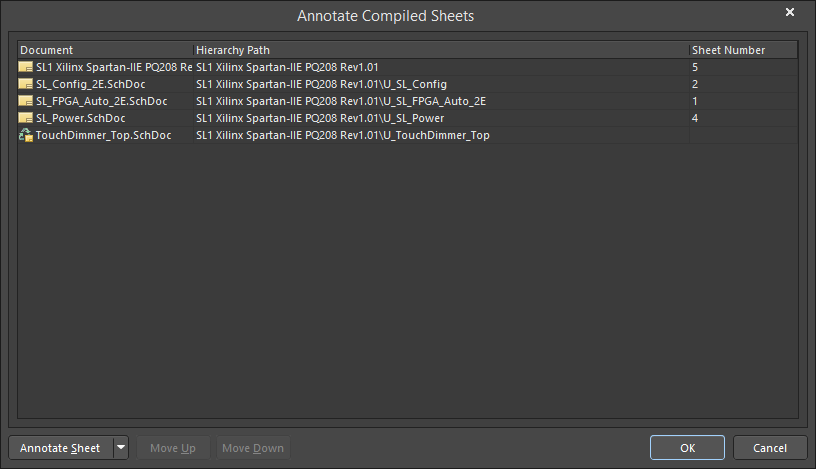
Annotating Compiled Sheet Options
Click on the Annotate Sheet drop-down to choose your Compiled Sheet Annotation Options.
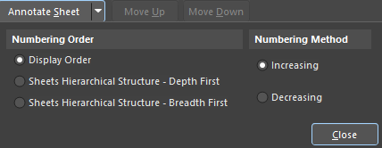
Numbering Order
- Display Order - the sheets are annotated in the order they are displayed.
- Sheets Hierarchical Structure - Depth First - the sheets are annotated from the top level into each branch. The top-level is annotated first and then the first branch under the top-level is annotated completely, the second branch and so on.
The Navigator view of your project shows the compiled (physical) representation of your sheets. When you annotate the sheets Depth First, you annotate each branch of the hierarchical structure at a time.
- Sheets Hierarchical Structure - Breadth First - the sheets are annotated according to their level in the hierarchy. The top-level is annotated first, all second levels are annotated next, and so on.
The Navigator view of your project shows the compiled (physical) representation of your sheets. When you annotate the sheets Breadth First, you annotate the sheets based on their position in the hierarchy meaning the top sheet is annotated first and then all of the second level sheets are annotated next.
Numbering Method
Choose Increasing or Decreasing to annotate your compiled sheets based on the Numbering Order chosen.
Annotating Compiled Sheets
After selecting your options:
- Click the Annotate Sheet button. The Sheet Number field will be updated to match your selections
- Click OK to accept your changes.
Custom Annotation of your Compiled Sheets
You can create custom names for your compiled sheets by typing directly into the Sheet Number field. You can use any combination of alphanumeric or non-alphanumeric characters. After entering your custom names, click OK to implement your custom annotation.
Using Compiled Sheet Annotation in your Board Level Annotation
Once you have annotated your Compiled Sheets, use the $SheetNumber keyword in your naming scheme when performing a Board Level Annotation to use this information in your annotation. If you have not annotated your compiled sheets, the Schematic Sheet numbering (Tools » Number Schematic Sheets) information will be used.
Using Compiled Sheet Annotation in your Project
Once you have annotated your compiled sheets, you can place the SheetNumber special string in your project to reference this information.
- The special string is always displayed; if null, then the parameter name is displayed.
- Place a special string where the value
=SheetNumberto use your Compiled Sheet Annotation values. You can use special strings in values of parameter properties, text strings, net labels, etc.
Board Level Annotation and Device Sheets
Device Sheets are portable and can be re-used between designs. In most cases, the names of the components in Device Sheets are limited to the scope of that sheet and require Board Level Annotation in order to be incorporated into the design in which they are placed.
Board Level Annotation is relevant to Device Sheets due to the fact that different Device Sheets included in one project can contain duplicate designators resulting in compilation errors. Board Level Annotation can resolve any conflicting naming with the changes saved to an *.Annotation file displayed under the Settings\Annotation Documents sub-folder.
Default Names for Compiled Components
Default Names are required to be able to distinguish between the different instances of the physical representations of components. These default names are displayed in your documents and are used if you have not performed a Board Level Annotation to annotate your compiled (physical) components. When you first launch the Board Level Annotate dialog, the default names are populated in the PCB Component Instance column.
Default naming of compiled components is also applicable for multi-channel designs that reference the same sheet in a project multiple times. This is done by either placing multiple sheet symbols that reference the same sheet in the Schematic Document or by including the Repeat keyword in the designator of a sheet symbol to instantiate a sheet multiple times.
While this makes it easy to repeat circuitry, it also presents a challenge in terms of annotation. In a multi-channel design, there can only be one logical instance of each component with its own unique designator no matter how many "copies" of it exist on the PCB. The Multi-Channel tab of the Project Options dialog (Project » Project Options) ensures that each channel is uniquely annotated with a default name based on Room Naming Style and Component Naming Designator Format.
Multi-Channel Tab
Rooms are regions that assist in the placement and annotation of components in multi-channel designs. More specifically, a channel on the schematic is an instance of a repeated sheet and on the PCB each channel is represented by a room. Once components have been assigned to a room, they move when the room is moved allowing separate channels to be easily controlled and identified.
Rooms play an important role in channel designations ensuring unique names.
Logical designators are assigned to the components in the Schematic Editor View. Physical designators are assigned to the components when they are placed in the PCB design or when you have performed a Board Level Annotation. In multi-channel designs, the logical designators for repeated channel components may be the same, but each component must have a unique physical designator in the PCB design. This can be accomplished by appending the Room Name to the component name as shown in the Component Naming field below.
The Multi-Channel tab of the Project Options dialog allows you to specify the Room Naming Style and the Component Naming Designator Format for your designs. By controlling the multi-channel designator format in this dialog, you control the mapping from the single logical component in the Schematic Editor View to the multiple physical instances on the PCB. The tab is essentially divided into two areas - Room Naming and Component Naming.

The Multi-Channel tab allows for flexible default naming formats in multi-channel designs.
Room Naming
Use the Room Naming Style drop-down to define the naming format you require for the rooms in your design. These rooms are created by default when you update the project schematics to the PCB. There are five styles available — two flat and three hierarchical.
|
Flat Room Name Formats |
Hierarchical Room Name Formats |
|---|---|
|
Flat Numeric With Names |
Numeric Name Path |
|
Flat Alpha With Names |
Alpha Name Path |
|
Mixed Name Path |
Hierarchical room names are formed by concatenating all channelized sheet symbol designators (ChannelPrefix + ChannelIndex) in the relevant channel path hierarchy.
As you select a room naming style from the list, the graphical representation is dynamically updated to reflect the naming convention that will appear in the design. The larger cross-hatch regions represent the upper-level channels (or Banks) and the shaded regions within represent the lower level channels. When the design is compiled, a room is created for each sheet in the design including each bank and each lower-level channel.
Use the Level Separator for Paths field to specify the required character/symbol for separating the path information when using the hierarchical naming styles. There are no restrictions on the character used for the level separator, however, a single non-alphanumeric character is easier to read.
Component Naming
There are several designator formats available for naming components. You can choose a format or define your own using valid keywords. Define the Component Naming format by selecting from the Designator Format drop-down list. There are eight predefined formats — five flat and three that can be used in a hierarchical context:
|
Flat Designator Formats |
|---|
|
$Component$ChannelAlpha |
|
$Component_$ChannelPrefix$ChannelAlpha |
|
$Component_$ChannelIndex |
|
$Component_$ChannelPrefix$ChannelIndex |
|
$ComponentPrefix_$ChannelIndex_$ComponentIndex |
|
Hierarchical Designator Formats |
|
$Component_$RoomName |
|
$RoomName_$Component |
|
$ComponentPrefix_$RoomName_$ComponentIndex |
The Flat Designator Formats name each component designator in a linear progression, starting from the first channel, avoiding the duplication of designators. The Hierarchical Designator Formats include the Room Name in the designator for a component. If the Room Naming Style chosen is one of the two possible flat styles, then the style for the component designator will also be flat. However, if a hierarchical style has been chosen for the Room Naming Style, the component designator will also be hierarchical since the path information will be included in the format.
Defining your own Designator Format
You can define your own component designator format by typing directly into the Designator Format field using valid keywords. Select from any combination of the following keywords to construct the format string.
|
Keyword |
Definition |
|---|---|
|
$RoomName |
Name of the associated room as determined by the style chosen in the Room Naming Style field |
|
$Component |
Component Logical Designator (e.g., U1) |
|
$ComponentPrefix |
Component Logical Designator Prefix (e.g., U for U1) |
|
$ComponentIndex |
Component Logical Designator Index (e.g., 1 for U1) |
|
$ChannelPrefix |
Logical Sheet Symbol Designator |
|
$ChannelIndex |
Index specified to distinguish between different channels |
|
$ChannelAlpha |
Channel Index expressed as an alpha character. This format is useful only if your design contains less than 26 channels in total or if you are using a hierarchical designator format |
Displaying Physical Names in your Documents
Your design is constructed in the Editor tab. Compiled Documents (physical representations of your design) are visible and can be accessed by clicking on the Compiled Document tab located along the bottom of the Schematic Document in the design window.

Examples of workspace tabs
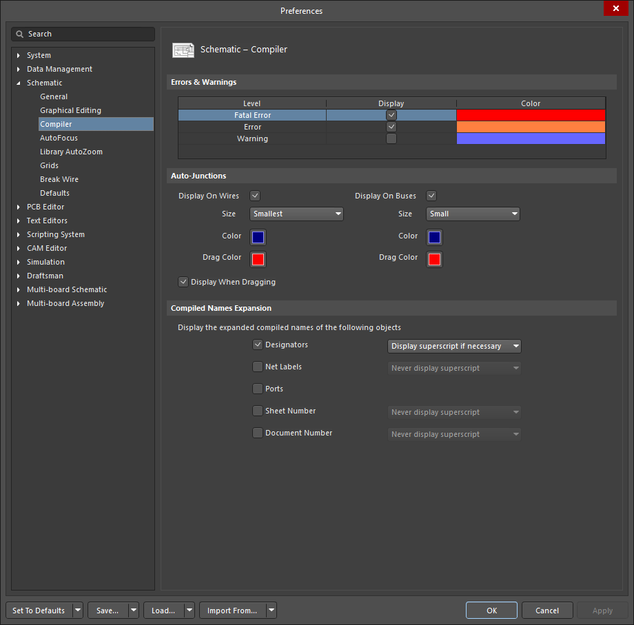
You can specify display preferences for the physical names in compiled documents on the Schematic - Compiler page of the Preferences dialog. In the Compiled Names Expansion region, select to expand the compiled (physical) names of Designators, Net Labels, Ports, Sheet Number and/or Document Number.
You also can use the associated drop-down to select how the objects are displayed. Choices include: Never display superscript (expanded names are never displayed), Always display superscript (expanded names are always displayed), or Display superscript if necessary (expanded names are only displayed if they are different from the source)
Use the Design » Update PCB Document command to initiate a transfer process that will automatically create a component class for each schematic sheet in the design, a room for each component class, and group the components in each class in their room ready for placement.
PCB Annotation
Positional Annotation in PCB
A key ingredient of good board design is component layout. In a large design, a component's position on the board may have no relationship to its designator. For example, R1 may end up on the opposite side of the board to R2. To make it easier to locate a component on the board, you can reassign the designators (re-annotate the board) positionally. To systematically assign designators in the PCB Editor based on their position, click Tools » Re-Annotate to open the Positional Re-Annotate dialog as shown below.
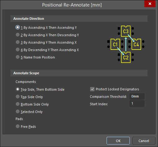
The Positional Re-Annotate dialog includes a graphical representation of each method.
Each component is identified by its bounding rectangle excluding strings. The components are sorted into a list and the list is renumbered in that order to create the new component designations. To compare two components in the X-direction, the left-side of the bounding rectangle is used. To compare two components in the Y-direction, the edge used depends upon the renumber direction: ascending-Y, use the bottom edge; descending-Y, use the top edge.
The Comparison Threshold option can be used as a buffer value when comparing two edges to determine if they are equal. For example, if two left-edges are within 75.0 mils of each other, and the comparison threshold is set to 100.0mil, then these two components are considered to be at the same X-position (left-edge). This allows for slightly misaligned components to be re-numbered in a logical order as shown in the image below. Here R27 is lower than the other resistors to keep it correctly annotated with the adjacent resistors (the Comparison Threshold was set to 10mils).
 A series of resistors that have been positionally re-annotated. Note that R27 has remained in the annotation sequence even though it is lower than the other resistors.
The Annotate Scope options also give control of the annotation process for boards with components mounted on both sides. For the Bottom Side of the board, components are re-annotated as if you are looking at the board flipped over. So, for the X-direction comparison on the back-side, the software actually uses the right edge of the bounding rectangle remembering that viewed from the back side, this edge would look like the left side.
If the Selected Only option is enabled, and re-annotation will result in a component in the selection set being given a designator that is a duplicate of an existing non-selected component, the non-selected component will have a _1 appended to its designator to ensure all designators remain unique.
Note that a rotated component is identified by the smallest bounding rectangle that encompasses the original bounding rectangle in its new rotated orientation as shown in the images below.

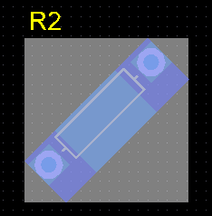 The image on the left shows the bounding rectangle for R2; the image on the right shows the new bounding rectangle when R2 is rotated.
An ASCII text file is generated (DesignName[Date][Time].WAS) in the same folder as the PCB document. The file lists initial and re-annotated designator values. Once a Re-Annotate has been performed on the PCB, you would typically pass these changes back to the Schematic using the Design » Update command. The *. WAS file also can be used to load the changes into the schematic if the PCB and schematic files are in different locations.
To prevent a component from having its designator re-assigned, enable the Protect Locked Designators checkbox in the Positional Re-Annotate dialog and ensure that the Strings locked icon is enabled in the associated Properties panel as shown below.
Controlling the Display of the Designator on the PCB
Extended Designator strings in a multi-channel design can be tedious to place in the PCB Editor. You can either choose naming options that result in a short name or display the original, logical component designation instead. For example, C30_CIN1 would display as C30. This would necessitate some other notation being added to the board to indicate the separate channels, such as a box being drawn around each channel on the component overlay.
You can select between Logical and Physical designator display on the PCB using the Designator Display drop-down in the Other region of the Properties panel in Board mode. If you choose to display the logical designators for components in a multi-channel design, these will be displayed on the PCB and in any output generated such as prints and Gerbers. The unique physical designators, however, are always used when generating a Bill of Materials.
Design Synchronization - Finalizing the Annotation Process
Direct Design Synchronization is the preferred method to keep your Schematic and PCB designators matching unless you do not have access to both the Schematic and the PCB editors. Design Synchronization compares the components and connectivity of the schematic directly to the PCB, producing a list of differences. A list of changes required to resolve these differences is generated as an ECO (Engineering Change Order). An ECO file describes the differences between the current design and the desired design and can be executed, updating the target and bringing the design into synchronization.
Forward Synchronization and Back Synchronization
The terms Forward Synchronization and Back Synchronization are specific ways of describing the direction that annotation and design changes are transferred during the synchronization of data. Visualizing a design flow that starts with, and is driven by, the schematic, Forward Synchronization is the process of updating changes made in the Schematic Editor forward to the PCB. Back Synchronization is the process of updating changes made in the PCB backward to the Schematic Editor.
Forward Synchronization
A few reasons why you would synchronize data from the Schematic to the PCB are:
- A new component is added in the Schematic Editor and is required in the PCB layout.
- You have annotated your schematic design for the first time or since your last design synchronization.
- In a multi-channel design, you have changed the Project Options to modify the physical (PCB) naming style.
- You have done a Board Level Annotation for the first time or since your last design synchronization.
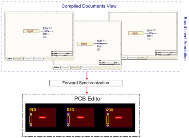
To Synchronize your Schematic Design forward to the PCB Design
Choose from one of the following methods to synchronize your Schematic design forward to your PCB design:
- Select Update PCB Document on the Design menu in the Schematic Editor. If any differences exist between these and the target PCB Document, the Engineering Change Order dialog opens with a list of modifications required to synchronize the PCB with the Schematic Design. Click Execute Changes to synchronize your design.
- Select Import Changes on the Design menu in the PCB Editor, which imports changes from the Schematic Documents to the PCB document.
Back Synchronization
Back Synchronization is done when you have annotated or changed your PCB design and you want to update the schematic design.
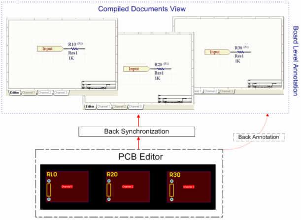
To Synchronize your PCB Design back to the Schematic Design
Choose from one of the following methods to synchronize your PCB design back to your schematic design:
-
in the PCB editor, select Update Schematics on the Design menu. By default, the Push Component Designator Changes to Annotation File (if any) option in the ECO Generation tab of the Project Options dialog is checked so that changes made in the PCB Editor will be pushed to the Annotation File only and, ultimately, Compiled Documents upon compilation. Uncheck this option to push changes to the source schematic document only (Editor view).
- From the schematic editor, select Tools » Annotation » Annotate Schematics then click the Back Annotate button in the Annotate dialog. Choose the WAS-IS file generated when re-annotating designators in the PCB environment.
- From the schematic editor, select Tools » Annotation » Board Level Annotate then click the Back Annotate button in the Board Level Annotate dialog. Choose the WAS-IS file generated when re-annotating designators in the PCB environment.
- From the schematic editor, select Tools » Annotation » Back Annotate Schematics. Choose the WAS-IS file generated when re-annotating designators in the PCB environment.
Traditional Methods of Design Synchronization
Altium NEXUS supports the traditional intermediate (netlist and WAS/IS) file approach for Design Synchronization. Forward Synchronization of annotation data can be done through the use of a netlist file and Back Synchronization can be done through the use of a WAS/IS file (listing what each designator WAS and what it now IS). The preferred method for synchronizing your design is Direct Design Synchronization.
Component Linking with Unique IDs
If you have re-annotated your design, the schematic component designators or the compiled component designators will no longer match the PCB component designators, so synchronization is required to successfully close off the design. Rather than relying on the designator itself as the key field that relates a schematic symbol to its equivalent PCB footprint, Altium NEXUS can maintain design synchronization through the Unique IDentifier (UID) system. The UID is a system-generated value that uniquely identifies the source component and matches each schematic component to the corresponding PCB component.
When a component is placed on a schematic sheet, it is automatically assigned a UID. The first time component information is transferred from source schematic documents to a blank PCB, the UID information from each schematic component is assigned to the corresponding PCB component.
Refactoring allows you to convert Device Sheets to Schematic Sheets and vice versa while maintaining the Unique ID of the sheet and its components. In addition, you can refactor (or move) subcircuits to other schematic sheets in the current project, maintaining the Unique ID of the subcircuit. The Refactor command is located on the Edit menu.
Altium NEXUS's synchronization feature, initiated by launching the Design » Update command, uses these UIDs to match each schematic component to its PCB equivalent. Design updates/changes can then be implemented using Engineering Change Orders (ECOs). An ECO lists all modifications required to implement changes to one or more design documents in order to satisfy the synchronization action requested. ECOs are used to affect design updates in a variety of situations, such as:
- SCH to PCB design updates.
- Performing Annotation updates to schematic component designators and compiled component designators.
- Implementing updates to parameters using the Parameter Manager (Tools » Parameter Manager).
- Updating parameter information with information stored in source libraries or a company database. Whenever you compare the schematic and PCB (such as when you select Design » Update), Altium NEXUS first matches components that share the same UID. When components are detected that do not share a UID, you are alerted and the application offers to attempt to match by designator. Until you have assigned a matching UID to both the schematic and the PCB, you will continue to get this message. Unique IDs and their correlation are managed in the Edit Component Links dialog (Project » Component Links).
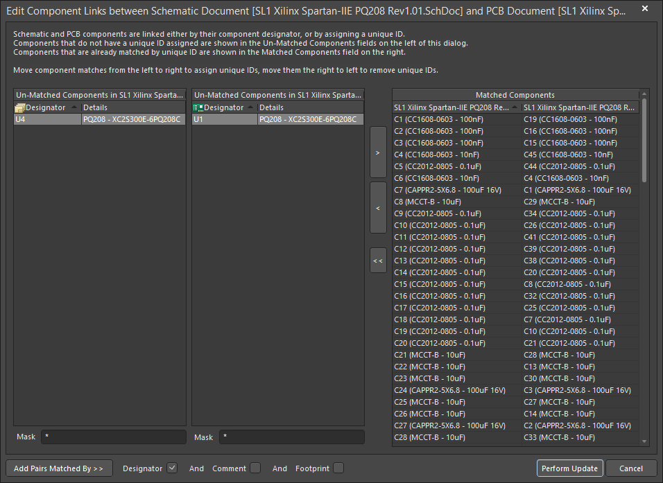
Note that the dialog can only be opened when a PCB document is active since UID changes are always applied to the PCB rather than the schematic. Use the dialog at any stage during the design to view the linking between the components to verify that components between documents are correctly matched, as well as to assign matching UIDs to components that are currently unmatched.