
Конфигурация стека слоев для трассировки с контролируемым импедансом
Когда трассировка становится частью контура
С увеличением скорости переключения устройств растут и требования к проектированию и производству печатных плат. Поскольку длина фронта переключения сигнала становится короче, чем длина трассы на печатной плате, которая его переносит, эту трассу следует рассматривать как часть контура. Трасса имеет импеданс, который называется характеристическим импедансом (Zo).
Лучший способ управлять воздействием этих дополнительных составляющих – сконструировать трассу так, чтобы характеристический импеданс был постоянным по всей длине – метод, называемый трассировкой с контролируемым импедансом.
Импеданс трассы определяется следующим:
- Площадью сечения трассы – определяется шириной, высотой (толщиной меди) и скосом краев трассы, созданным в процессе травления.
- Расстояние от трассы до опорной плоскости (или плоскостей) – возвратный путь энергии сигнала так же важен, как и путь сигнала. Этот возвратный путь следует пути сигнала на прилегающей опорной плоскости (плоскостях).
- Свойства окружающих материалов – энергия сигнала не содержится внутри проводящего материала трассы, из-за скин-эффекта она также проходит по диэлектрическому материалу, который окружает трассу. Диэлектрическая проницаемость этого материала характеризует, насколько диэлектрик влияет на поток этой энергии.

 Калькулятор импеданса Simbeor рассчитывает ширину, необходимую для соответствия определенному импедансу.
В обычном проекте платы конструктор указывает ширину/зазоры для трассы, чтобы удовлетворить требованиям к току/напряжению.
В проекте с контролируемым импедансом конструктор указывает импеданс, а не ширину трассы. С помощью встроенного калькулятора импедансов Simbeor®, Layer Stack Manager редактора плат рассчитывает ширину трассы, необходимую для достижения указанного импеданса.
Расчет импеданса
Ширину трассы, необходимую для достижения определенного импеданса, можно рассчитать в рамках профиля импеданса, на вкладке Impedance в Layer Stack Manager.
Входными данными расчета являются:
- Значения Target Impedance (Целевой импеданс) и Target Tolerance (Целевой допуск), который вы указываете на вкладке Impedance.
- Настройки материала, указанные на вкладке Stackup, в том числе:
- толщина сигнального слоя;
- толщина окружающих диэлектрических слоев (расстояния от опорных слоев);
- свойства диэлектрических материалов (диэлектрическая проницаемость Dk и тангенс угла диэлектрических потерь Df).
Когда эти значения заданы корректно, у калькулятора импедансов достаточно информации для расчета следующего:
- Ширина трассы
- Расчетный импеданс (Z)
- Отклонение импеданса (Z Deviation)
- Задержка на распространение (Tp)
- Индуктивность на единицу длины
- Емкость на единицу длины
Поддерживаемые структуры
- Микрополосковая линия
- Симметричная полосковая линия
- Несимметричная полосковая линия
- Одиночные и дифференциальные копланарные структуры
- Множество прилегающих друг к другу слоев, с различными диэлектрическими свойствами
- Моделирование шероховатости поверхности проводника
Расчетные значения отображаются в разделе Transmission Line панели Properties, когда в Layer Stack Manager выбрана вкладка Impedance, как показано ниже.
.") Профиль импеданса 50Ω, определенный для одиночных цепей на верхнем слое. Наведите курсор мыши на изображение, чтобы увидеть настройки этого же профиля для слоя L3 (изображение предоставлено FEDEVEL Open Source, www.fedevel.com).
Профиль импеданса 50Ω, определенный для одиночных цепей на верхнем слое. Наведите курсор мыши на изображение, чтобы увидеть настройки этого же профиля для слоя L3 (изображение предоставлено FEDEVEL Open Source, www.fedevel.com).
Создание и настройка профиля импеданса
- В Layer Stack Manager переключитесь на вкладку Impedance, как показано выше.
- Нажмите кнопку
 (или кнопку
  , если уже есть созданные профили), чтобы добавить новый профиль.
 - Задайте требуемые параметры Type, Target Impedance и Target Tolerance импеданса в панели Properties. Описание Description является опциональным, оно будет отображаться вместе с названием профиля импеданса.
- Таблица слоев разделена на две области – слева показаны слои в стекапе, для каждого сигнального слоя в стекапе показан слой в области профилей импедансов справа. Используйте флажки слоев в области профилей для включения расчета импеданса для этого слоя.
- Выберите включенный слой в области профилей. В стеке слоев будут затенены все слои, кроме тех, которые используются для расчета импеданса для выбранного сигнального слоя (как показано на изображении выше). Измените опорные слои этого слоя в столбцах Top Ref и Bottom Ref. Обратите внимание, что опорными слоями могут быть экранные и сигнальные слои.
- Включите флажок профиля импеданса для всех остальных слоев, на которых будет расположена трассировка с этим импедансом, и настройте опорные плоскости. Наведите курсор мыши на изображение выше, чтобы увидеть профиль импеданса S50 для слоя L3.
Настройки ширины и зазора
На основе целевого импеданса и целевого допуска система вычисляет ширину трассы. Довольно часто расчетной шириной трассы будет значение, которое нельзя заказать, например 0,0683 мм. Производитель сообщит, какие толщины материалов доступны и какой точности они могут достичь для ширины трасс. Затем, начиная с желаемых значений, проверяется влияние на расчетные значения импеданса размеров тех значений, которые доступны.
Для поддержки проверки и подстройки значений калькулятор импедансов поддерживает прямые и обратные вычисления. По умолчанию используются прямые вычисления (ввод импеданса, по которому система вычисляет ширину). Иконка  обозначает расчетную переменную.
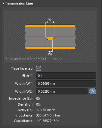
 составляет 94,6 мкм. На изображении справа показан обратный расчет, при котором задана ширина (W1) 95 мкм.")
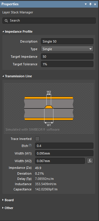 При прямом расчете для целевого импеданса 50Ω расчетная ширина (W1) составляет 94,6 мкм. На изображении справа показан обратный расчет, при котором задана ширина (W1) 95 мкм.
Чтобы провести обратный расчет и изучить различные значения ширины трасс для выбранного слоя, введите новое значение Width (W1) и нажмите клавишу Enter. Расчетные значения будут обновлены в соответствии с изменением ширины. Нажмите кнопку , чтобы вернуться в режим прямого расчета. Введите новое значение в поле Width (W2), чтобы изменить значение Etch.
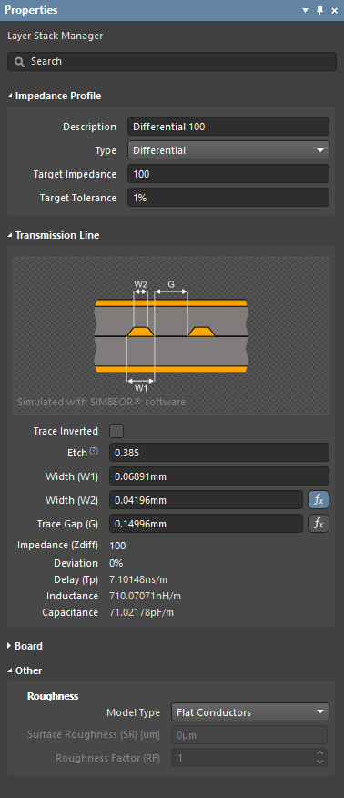
Чтобы изучить результаты линии передачи дифференциальной пары, укажите расчетную переменную (ширину трассы Trace Width или зазор Trace Gap), нажав соответствующую кнопку . Измените прочие переменные, чтобы изменить Target Impedance, либо измените Target Impedance, чтобы изучить влияние на другую переменную.
Коэффициент подтрава
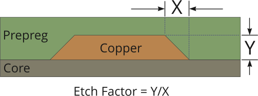
Сигнальные трассы на плате формируются путем травления ненужной меди. Поскольку травящее вещество начинает вытравливать медь с поверхности, медь на поверхности проводит больше времени в контакте с этим веществом. В результате у краев конечной трассы будет скос, что уменьшит ее площадь сечения, как показано на изображении ниже.
Площадь меди, потерянной в результате травления (с обеих сторон) = X * Y
Величина скоса называется коэффициентом подтрава (Etch Factor), где:
Etch Factor = Y/X
Если Y = X, то Etch Factor = 1
Изображение в панели Properties:
 Наведите курсор мыши на символ ?, чтобы увидеть формулу.
Стандартное определение коэффициента подтрава – это отношение толщины трассы к величине подтрава. Это дает следующую формулу:
Etch Factor = T/[0.5(W1-W2)]
Недостатком такого подхода является то, что при отсутствии подтрава (т.е. при вертикальных краях трассы) необходимо было вводить значение inf (бесконечность) для коэффициента травления. Для упрощения указания величины травления формула была инвертирована, поэтому для указания того, что подтрав отсутствует, можно ввести значение 0 (ноль).
Etch = [0.5(W1-W2)]/T
Ориентация меди
Еще одним фактором производства, который влияет на коэффициент травления, является ориентация меди. Трассы на плате формируются путем травления ненужной меди из сплошного листа меди на диэлектрической подложке. Ориентация меди определяет направление, в котором медь выступает от этой подложки. Вы также можете воспринимать это как направление травления меди, сверху или снизу.

 Включите опцию Trace Inverted для переключения ориентации меди с Above на Below.
Шероховатость поверхности проводника
Поверхность каждого проводящего слоя платы имеет некоторую шероховатость. При изготовлении печатной платы поверхность проводящих слоев обрабатывается для увеличения шероховатости и улучшения адгезии между проводящим и диэлектрическим слоями. Шероховатость поверхности значительно влияет на импеданс проводника при скоростях переключения выше 10 ГБ/с. В результате обширных исследований и анализа отраслевые эксперты пришли к выводу, что шероховатость поверхности можно смоделировать с помощью поправочного коэффициента шероховатости, полученного из значений Surface Roughness (Шероховатость поверхности) и Roughness Factor (Коэффициент шероховатости).
Настройки Roughness доступны в режиме Layer Stack Manager панели Properties. Эти параметры используются только для проводящих слоев.
 Шероховатость поверхности учитывается при расчете характеристического импеданса.
Шероховатость:
- Model Type (Тип модели) – предпочтительная модель для расчета влияния шероховатости поверхности (см. статьи ниже для получения более подробной информации по различным моделям). Применяется ко всем проводящим слоям в сабстеке.
- Surface Roughness (Шероховатость поверхности) – значение шероховатости поверхности (доступное производителю). Введите значение от 0 до 10µm, по умолчанию – 0.1µm
- Roughness Factor (Коэффициент шероховатости) – характеризует ожидаемое максимальное увеличение потерь в проводнике из-за эффекта шероховатости. Введите значение от 1 до 100, по умолчанию – 2.
Для дальнейшего чтения
- Practical methodology for analyzing the effect of conductor roughness on signal losses and dispersion in interconnects: Y. Shlepnev, C. Nwachukwu, DesignCon2012.
- Unified approach to interconnect conductor surface roughness modelling: Y. Shlepnev, 2017 IEEE 26st Conference on Electrical Performance of Electronic Packaging and Systems (EPEPS2017)
Поддержка структур копланарных линий передач
Калькулятор импедансов в Layer Stack Manager поддерживает одиночные и дифференциальные копланарные структуры. Создайте новый профиль импеданса и выберите Single-Coplanar или Differential-Coplanar из выпадающего списка Type профиля импедансов.

Работа с копланарными структурами:
- Как со стандартными одиночными и дифференциальными импедансами, значения каждой переменной вычисляются автоматически исходя из заданных пользователем значений Target Impedance и Target Tolerance и физических свойств слоев платы. Эти автоматически вычисленные значения можно изменить, введя новые значения в текстовые поля в режиме Layer Stack Manager панели Properties.
- Чтобы задать сигнальные цепи, которые вы хотите трассировать как копланарную структуру, настройте правило проектирования Routing Width (или Differential Pairs Routing), включив опцию Use Impedance Profile и выбрав нужный копланарный профиль импеданса.
- Для копланарных структур требуется опорная плоскость по обеим сторонам от сигнальной трассы. Ее можно создать путем размещения полигона или добавления прошивки переходными отверстиями с помощью команды Add Shielding to Net (подробнее об этом ниже). Если вы размещаете полигон, разделение между этим полигоном и сигнальной трассой определяется значением Clearance (S), определенным калькулятором импедансов Simbeor (отображается в панели Properties, как показано на изображениях выше и ниже). Настройте правило проектирования Clearance для управления зазором между опорной плоскостью и сигнальной трассой ( показать изображение).
-
Распространенной практикой является добавление "ограждения" из переходных отверстий вдоль каждой из сторон сигнальной трассы, если копланарная структура заземлена. Для этого используйте команду Tools » Via Stitching/Shielding » Add Shielding to Net в редакторе плат. Помимо размещения переходных отверстий, вы можете включить опцию Add shielding copper, чтобы эта команда также разместила полигон вокруг сигнальной трассы и закрыла им переходные отверстия, как показано на правом изображении ниже.
► Узнайте больше об Экранировании с помощью переходных отверстий
 показать изображение
 . Используйте этот зазор в настройке расстояния экранирования с помощью переходных отверстий.")
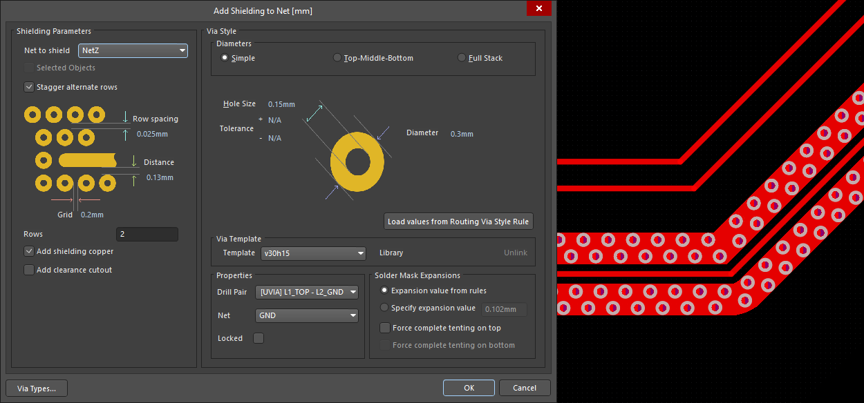 Калькулятор импедансов определяет свойства и зазоры сигналов (первое изображение). Используйте этот зазор в настройке расстояния экранирования с помощью переходных отверстий.
Выбор материала слоя
В проекте с контролируемым импедансом очень важен выбор материалов, используемых в стекапе слоев.
Например, наиболее распространенным материалом, используемым для изготовления плат, является стеклотекстолит, армированный эпоксидной смолой, с медной фольгой, наклеенной на каждую сторону. Плотность переплетения стекловолокна влияет на значение и постоянство диэлектрической проницаемости Dk и тангенса угла потерь Df. Вокруг плетеной стеклоткани находится смола – процент используемой смолы также оказывает влияние на характеристики материала.
Существует множество видов плетений стекловолокна. Для обеспечения предсказуемости и необходимых характеристик материалов на основе стекловолокна, используемых при изготовлении печатных плат, IPC разработал стандарт на плетения:
IPC standard IPC-4412B: Specification for Finished Fabric Woven from "E" Glass for Printed Boards
Библиотека материалов
Как конструктор, вы можете изменять свойства материалов непосредственно в Layer Stack Manager либо вы можете выбрать материал из библиотеки Altium Material Library.
Всю библиотеку можно просмотреть (и добавить) в диалоговом окне Altium Material Library (Tools » Material Library).
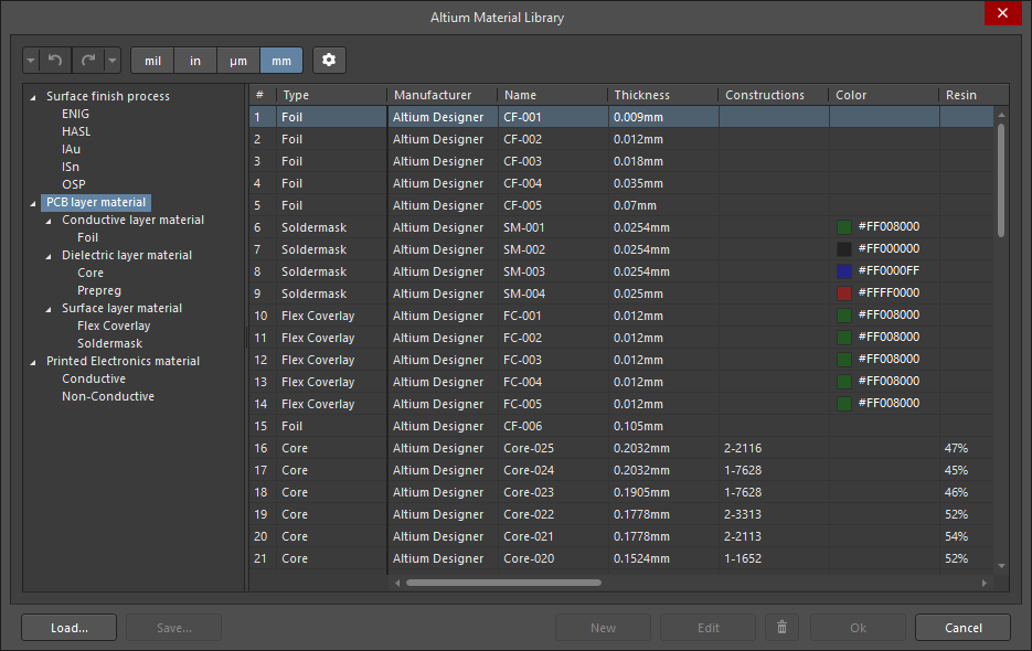
Материалы разбиты по категориям использования, которые доступны в виде древовидной структуры в левой части диалогового окна. Далее каждая категория использования разделяется на функциональные категории, например Conductive layer material, Dielectric layer material и Surface Layer Material в категории PCB layer material.
Добавление, сохранение и загрузка материалов
Когда в дереве навигации выбрана определенная категория материалов, в библиотеку может быть добавлен новый материал. Могут быть загружены материалы, определенные во внешней библиотеке (кнопка Load), а пользовательские материалы, которые были добавлены в диалоговое окно Altium Material Library, могут быть сохранены в пользовательскую библиотеку (кнопка Save). Будут сохранены только материалы, определенные пользователем.
Добавление пользовательских свойств в материал
В материалы, заданные в библиотеке (материалы по умолчанию и заданные пользователем), могут быть добавлены пользовательские свойства. Чтобы добавить пользовательское свойство, сначала выберите нужный узел в дереве слева, чтобы определить, в какие материалы это свойство будет добавлено, и нажмите кнопку ![]() , чтобы открыть диалоговое окно Material Library Settings.
, чтобы открыть диалоговое окно Material Library Settings.
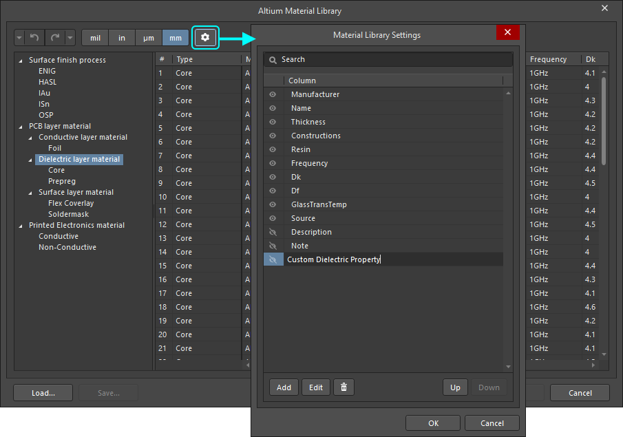
Затем нужное значение может быть добавлено в выбранный материал в диалоговом окне Altium Material Library. Для этого выберите строку и нажмите кнопку Edit.
Применение профиля импеданса к трассировке
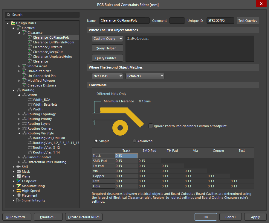
В трассировке с контролируемым импедансом крайне важна настройка ширины трасс для обеспечения нужного импеданса, что означает, что ширина трассы может отличаться для различных слоев. Это управляется путем назначения профиля импеданса вместо определенной ширины трассы при настройке правила в PCB Rules and Constraints Editor (Design » Rules). После этого система автоматически определит ширину для каждого слоя.
Выбор нужного импеданса осуществляется в правиле проектирования Routing Width (для отдельных цепей) или Differential Pairs Routing.
 Это правило проектирования применено к классу цепей DRAM. Профиль импеданса S50 определяет ширину трасс в соответствии со слоем, на котором они будут трассироваться.
- Включите опцию Use Impedance Profile в разделе Constraints правила проектирования. В выпадающем списке будут представлены все доступные профили импедансов подходящего типа (одиночные или дифференциальные). Выберите профиль, необходимый для цепей, для которых предназначено правило проектирования.
- Когда выбран профиль импеданса, значение ширины из профиля будет применено к настройке Preferred Width в правиле. Это применяется к каждому сигнальному слою, включенному в профиле; все остальные сигнальные слои, которые не включены в этом профиле, будут удалены.
- Когда применен профиль импеданса, настройку Preferred Width больше нельзя изменить. Настройки Min Width и Max Width всё ещё доступны для редактирования, задайте им подходящие большие/меньшие значения.
- Цепи можно трассировать в интерактивном режиме, как обычно.
► Узнайте больше о Трассировке с контролируемым импедансом