Working with the Differential Pairs Routing Design Rule on a PCB in Altium NEXUS
Rule category: Routing
Rule classification: Unary
Summary
This rule defines the routing width of each net in a differential pair, and the clearance (or gap) between the nets in that pair. Differential pairs are typically routed with specific width-gap settings to deliver the required single-ended and differential impedance needed for that net-pair.
Constraints
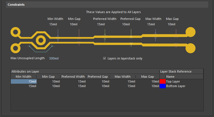
 Default constraints for the Differential Pairs Routing rule.
- Min Width - specifies the minimum permissible width to be used for tracks when routing the differential pair.
- Min Gap - specifies the minimum permissible clearance between primitives on different nets within the same differential pair.
- Preferred Width - specifies the preferred width to be used for tracks when routing the differential pair.
- Preferred Gap - specifies the preferred clearance between primitives on different nets within the same differential pair.
- Max Width - specifies the maximum permissible width to be used for tracks when routing the differential pair.
- Max Gap - specifies the maximum permissible clearance between primitives on different nets within the same differential pair.
- Max Uncoupled Length - specifies the value for the maximum permissable uncoupled length between positive and negative nets within the differential pair.
- Layers in layerstack only - allows you to display and edit width-gap constraints for only the defined signal layers in the layer stack. When enabled, only the layers in the stack will be displayed in the Layer Attributes Table. When disabled, all signal layers will be displayed.
- Layer Attributes Table - displays all signal layers or only those defined in the layer stack as controlled by the Layers in layerstack only option. The minimum, maximum and preferred width and gap constraints are displayed, as well as other layer-specific information. The width and gap fields can be set globally for all layers by defining values using the controls to the right of the graphic, or individually by typing width and gap values directly into the table.
How Duplicate Rule Contentions are Resolved
All rules are resolved by the priority setting. The system goes through the rules from highest to lowest priority and picks the first one whose scope expression matches the object(s) being checked.
Rule Application
Online DRC, Batch DRC, interactive routing (and re-routing), autorouting, interactive length tuning (Min Gap is applied), and when interactively modifying the pair, such as sliding a track segment of one of the nets in the pair.
Tips
- While the width of each net in a differential pair is monitored by the applicable Differential Pairs Routing rule (and not by a Width rule), clearance checking between the nets in that pair is still governed by the an applicable Clearance design rule. In other words, a Clearance rule must be defined that targets the differential pair (on the specific layer where needed) with its connective checking mode set to Same Differential Pair, and whose clearance is set to be equal to, or lower than, the value for the Min Gap constraint defined for that layer as part of the applicable Differential Pairs Routing rule.
- The clearance from a net in a differential pair to any other electrical object that is not a part of the pair is monitored by the applicable Clearance rule.
- While the optimal width-gap settings may be achievable for most of the board, there will often be areas, such as under a BGA component, where smaller and tighter width-gap settings must be used. As well as switching the Width-Gap settings interactively, this requirement can also be achieved by defining multiple differential pair routing rules - a lower-priority rule that targets the differential pair across the board, and a higher-priority rule that targets the differential pair in specific areas. You then target the differential pair in a specific area by defining a Room Definition rule and use that room as part of the scope of a differential pair routing rule.
-
Differential Pair classes, for use in rule scoping, can be defined on the schematic.
