Rule category: Routing
Rule classification: Unary
Summary
This rule defines the width of tracks placed on the copper (signal) layers.
Constraints
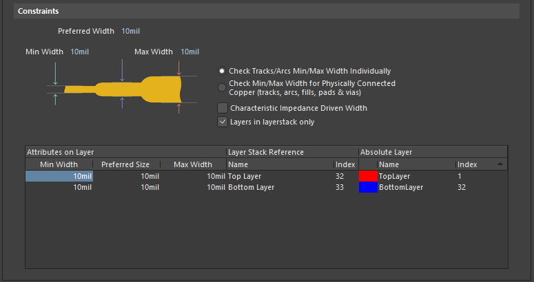
 Default constraints for the Width rule.
- Min Width - specifies the minimum permissible width to be used for tracks when routing the board.
- Preferred Width - specifies the preferred width to be used for tracks when routing the board.
- Max Width - specifies the maximum permissible width to be used for tracks when routing the board.
The values specified for Min Width, Preferred Width, and Max Width will apply to all signal layers.
- Check Tracks/Arcs Min/Max Width Individually - checks individual widths of tracks and arcs fall within the minimum and maximum range.
- Check Min/Max Width for Physically Connected Copper (tracks, arcs, fills, pads & vias) - checks the width of routed copper formed by a combination of tracks, arcs, fills, pads & vias falls within the minimum and maximum range.
- Characteristic Impedance Driven Width - if the design needs to be routed to strict impedance requirements, ensure that this option is enabled. When the rule is configured in this mode, the routing width required on each routing layer is calculated based on the specified impedance, using the appropriate equation (Microstrip or Stripline) and the physical parameters of the layer stack. Once the rule is defined, as you route a net that falls under the scope of the rule, the track width will automatically be set to the width required to meet the specified impedance for that layer. The Min/Preferred/Max Width constraints change to the following impedance-based incarnations:
- Min Impedance - specifies the minimum permissible impedance to be observed when routing the board (default =
50 ohms).
- Preferred Impedance - specifies the preferred impedance to be observed when routing the board (default =
50 ohms).
- Max Impedance - specifies the maximum permissible impedance to be observed when routing the board (default =
50 ohms).
- Layers in layerstack only - allows you to display and edit the width constraints for just the defined signal layers in the layer stack. When enabled, only the layers in the stack will be displayed in the Layer Attributes Table. When disabled, all signal layers will be displayed.
- Layer Attributes Table - displays all signal layers or only those defined in the layer stack, as controlled by the Layers in layerstack only option. The minimum, maximum and preferred routing widths are displayed, as well as other layer-specific information. The routing width fields can be set globally by defining a value in the individual width constraint fields, or individually by typing a width value directly into the table. When the Characteristic Impedance Driven Width option is enabled, the required width entries will be automatically calculated and entered for each layer in the table. They can not be defined on an individual basis while in this mode.
When defining values for the minimum, maximum and preferred routing widths, the Layer Attributes Table will highlight any invalid entries by using red text. This could happen, for example, when you specify a minimum constraint value that is greater than the maximum constraint value. The incorrect rule definition is further highlighted by the rule name becoming red in both the folder-tree pane and the respective summary lists, in the PCB Rules and Constraints Editor dialog.
How Duplicate Rule Contentions are Resolved
All rules are resolved by the priority setting. The system goes through the rules from highest to lowest priority and picks the first one whose scope expression matches the object(s) being checked.
Rule Application
The Preferred Width setting is obeyed by the Autorouter.
The Min Width and Max Width settings are obeyed by the Online DRC and Batch DRC. They also determine the range of permissible values that can be used during interactive routing (press Tab key while routing to change the trace width within the defined range, through the Properties panel). If a value is entered outside of this range, it will automatically be clipped.
Tips
- The width of each net in a differential pair is monitored by the applicable Differential Pairs Routing rule.
- The impedance equations used for calculating the impedance and trace width are accessed from the Layer Stack Manager dialog, by pressing the Impedance Calculation button. The subsequent dialog that appears - the Impedance Formula Editor dialog - contains impedance calculators for both Microstrip and Stripline impedance calculations. Default equations are in place to calculate the impedance and the required trace width in order to satisfy that impedance when routing (as shown below). These equations can be modified if required.
MicrostripExpandСвернуть
- Calculated Impedance - the default formula is:
(60/SQRT(Er*(1-EXP(-1.55*(0.00002+TraceToPlaneDistance)/TraceToPlaneDistance))))*LN(5.98*TraceToPlaneDistance/(0.8*TraceWidth+TraceHeight))
- Calculated Trace Width - the default formula is:
((5.98*TraceToPlaneDistance)/EXP(CharacteristicImpedance/(60/SQRT(Er*(1-EXP(-1.55*(0.00002+TraceToPlaneDistance)/TraceToPlaneDistance)))))-TraceHeight)/0.8
Note that if the plane layer is not adjacent to the signal layer then the nearest plane layer will be used in the calculations.
StriplineExpandСвернуть
- Calculated Impedance - the default formula is:
(80/SQRT(Er))*LN((1.9*(2*TraceToPlaneDistance+TraceHeight)/(0.8*TraceWidth+TraceHeight)))*(1-(TraceToPlaneDistance/(4*(PlaneToPlaneDistance-TraceHeight-TraceToPlaneDistance))))
- Calculated Trace Width - the default formula is:
((1.9*(2*TraceToPlaneDistance+TraceHeight))/(EXP((CharacteristicImpedance/(80/SQRT(Er)))/(1-(TraceToPlaneDistance/(4*(PlaneToPlaneDistance-TraceHeight-TraceToPlaneDistance))))))-TraceHeight)/0.8
Note that if the plane layers are not adjacent to the signal layer then the nearest plane layers will be used in the calculations. Note also that an offset stripline configuration is not supported.
