
Configuring PCB Via Object Properties in Altium NEXUS
Created: октября 22, 2019 | Updated: апреля 10, 2021
| Applies to versions: 3.0, 3.1 and 3.2
Вы просматриваете версию 3.2. Для самой новой информации, перейдите на страницу Configuring PCB Via Object Properties in Altium NEXUS для версии 4
Parent page: Via
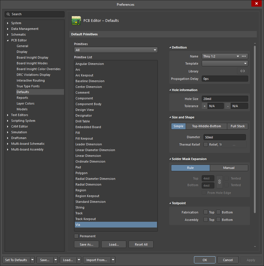
PCB Editor object properties are definable options that specify the visual style, content and behavior of the placed object. The property settings for each type of object are defined in two different ways:
- Pre-placement settings – most Via object properties, or those that can logically be pre-defined, are available as editable default settings on the PCB Editor - Defaults page of the Preferences dialog (accessed from the
 button at the top-right of the design space). Select the object in the Primitive List to reveal its options on the right.
- Post-placement settings – all Via object properties are available for editing in the Via dialog and the Properties panel when a placed Via is selected in the design space.
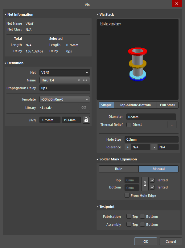

Net Information
- Net Name - the name of the selected net.
- Net Class - the name of the selected net class.
- Total
- Length - the total Signal Length. The Signal Length is the accurate calculation of the total node-to-node distance. Placed objects are analyzed to resolve stacked or overlapping objects and wandering paths within pads, and via lengths are included. The Pin Package Length is also included if it has been defined for the pad(s). If the net is not completely routed, the Manhattan (X + Y) length of the connection line is also included. For more information regarding Signal Length and its applications, see the PCB - Nets page.
- Delay - the delay of the routed segments of the Total Length. Includes the Pad and Via Propagation Delay values if they have been defined for the pads and vias.
- Selected
- Length - the total length sum of the selected object(s).
- Delay - the total delay of the selected object(s). Includes selected Pad and Via Propagation Delay values if they have been defined for the pads and vias.
Definition
- Net - use to choose a net for the via. All nets for the active board design will be listed in the drop-down list. Select No Net to specify that the via is not connected to any net. The Net property of a primitive is used by the Design Rule Checker to determine if a PCB object is legally placed. Alternatively, you can click on the Assign Net icon (
 ) to choose an object in the design space - the net of that object will be assigned to selected via(s).
 - Name - when one or more via is/are selected, the via names are displayed by clicking the drop-down, which lists all of the via spans defined in the Layer Stack. All vias used on the board must be one of the via spans defined in the Layer Stack.
- Template - displays the current template for the via. Use the drop-down to select another template. If there is an associated Library, that library will be displayed.
- Library - displays the via template contained in the current library. If a via is placed from a Pad Via Library (*.PvLib), it will include the name of that library in this field. Once placed, the
 icon becomes enabled, which indicates that the properties of the placed via are defined in the Library, and are no longer editable. If the
  icon is not enabled, the contents can still be edited.
 - Propagational Delay - this field lists the propagation delay, which is the amount of time it takes for the head of the signal to travel from the sender to the receiver.
Location (Properties panel only)
- (X/Y)
- X (first field) - this field shows the current X position of the center of the via relative to the current origin. Edit the value in the field to change the position of the via relative to the current origin. The value can be entered in either metric or imperial; include the units when entering a value whose units are not the current default. Default units (metric or imperial) are determined by the Units setting in the Other region of the Properties panel in Board mode (accessed when no objects are selected in the design space) and are used if the unit is not specified.
- Y (second field) - this field shows the current Y position of the center of the via relative to the current origin. Edit the value in the field to change the position of the via relative to the current origin. The value can be entered in either metric or imperial; include the units when entering a value whose units are not the current default. Default units (metric or imperial) are determined by the Units setting in the Other region of the Properties panel in Board mode (accessed when no objects are selected in the design space) and are used if the unit is not specified.
Hole Information
- Hole Size - this field displays the current hole size for the via. The value specifies the diameter of the hole (as a round, square or slotted shape) in mils or mm to be drilled in the via during fabrication. The hole size can be set from 0 to 1000mil and can be set larger than the via to define (copper free) mechanical holes. Edit the value in this field to change the via hole size. The value can be entered in either metric or imperial; include the units when entering a value whose units are not the current default. Default units (metric or imperial) are determined by the Units setting in the Other region of the Properties panel in Board mode (accessed when no objects are selected in the design space) and are used if the unit is not specified.
- Tolerance - setting hole tolerance attributes can help determine the fits and limits of your board. Specify the minimum (-) and maximum (+) tolerances for the hole. There is no default hole tolerance value in Altium NEXUS.
Size and Shape
- Simple - select to choose a simple via.
- Diameter - enter the required diameter of the via. The via diameter is the same on all layers.
- Thermal Relief - check the box to enable thermal relief to reduce heat conductivity. Once checked, click
 to open the Polygon Connect Style dialog in which you can choose the style of the connection: Relief Connect, Direct Connect, or No Connect.
- Top-Middle-Bottom - select to choose different diameters for the top layer, all internal signal layers, and Bottom Layer.
- Displayed Layer(s) - click on a displayed layer to configure vias for that layer. The selected layer is highlighted.
- Diameter - click the drop-down then enter the required diameter of the via for the selected layer.
- Thermal Relief - check the box to enable thermal relief to reduce heat conductivity. Once checked, click to open the Polygon Connect Style dialog in which you can choose the style of the connection: Relief Connect, Direct Connect, or No Connect.
- Full Stack - select to choose a Full Stack via object.
- Displayed Layer(s) - click on a displayed layer to configure vias for that layer. The selected layer is highlighted.
- Diameter - click the drop-down then enter the required diameter of the via for the selected layer.
- Thermal Relief - check the box to enable thermal relief to reduce heat conductivity. Once checked, click to open the Polygon Connect Style dialog in which you can choose the style of the connection: Relief Connect, Direct Connect, or No Connect.
Solder Mask Expansion
- Rule - select to have the solder mask expansion for the via follow the defined value in the applicable Solder Mask Expansion design rule.
- Top
- Tented - check if it desired for any solder mask settings in the solder mask expansion design rules to be overridden, which results in no opening in the solder mask on the top layer of this via and is therefore tented. Disable this option and this via is affected by a solder mask expansion rule or specific expansion value.
- Bottom
- Tented - check if it desired for any solder mask settings in the solder mask expansion design rules to be overridden, which results in no opening in the solder mask on the bottom layer of this via and is therefore tented. Disable this option and this via is affected by a solder mask expansion rule or specific expansion value.
- Top
- Manual - select to override the applicable design rule and specify the solder mask expansion value for the via.
- Top - enter the top layer solder mask expansion value. The value can be entered in either metric or imperial; include the units when entering a value whose units are not the current default. Default units (metric or imperial) are determined by the Units setting in the Other region of the Properties panel in Board mode (accessed when no objects are selected in the design space) and are used if the unit is not specified. This field is accessible only if Tented is not enabled.
- Tented - check if it desired for any solder mask settings in the solder mask expansion design rules to be overridden, which results in no opening in the solder mask on the top layer of this via and is therefore tented. Disable this option and this via is affected by a solder mask expansion rule or specific expansion value.
-
 - you can enter Bottom measurement and Tented options if Bottom layer Solder Mask Expansion values are required. Click
  to disable Bottom layer options if they are not required.
 - Bottom - enter the bottom layer solder mask expansion value. The value can be entered in either metric or imperial; include the units when entering a value whose units are not the current default. Default units (metric or imperial) are determined by the Units setting in the Other region of the Properties panel in Board mode (accessed when no objects are selected in the design space) and are used if the unit is not specified. This field is accessible only if the link icon is set to and the Tented option is not enabled.
- Tented - check if it desired for any solder mask settings in the solder mask expansion design rules to be overridden, which results in no opening in the solder mask on the bottom layer of this via and is therefore tented. Disable this option and this via is affected by a solder mask expansion rule or specific expansion value.
- From Hole Edge - when enabled, the Solder Mask opening will follow the shape of the via. The mask is therefore independent of via shape and size and is scaled from both the hole size and shape. For example, a via with a square hole will create a square mask opening that matches the hole dimensions, as well as the assigned expansion value. Also note that a via's expansion mask opening size will track any changes in the hole size.
- Top - enter the top layer solder mask expansion value. The value can be entered in either metric or imperial; include the units when entering a value whose units are not the current default. Default units (metric or imperial) are determined by the Units setting in the Other region of the Properties panel in Board mode (accessed when no objects are selected in the design space) and are used if the unit is not specified. This field is accessible only if Tented is not enabled.
Notes on Tenting
Partial and complete tenting of vias can be achieved by defining an appropriate value for Solder Mask Expansion. This expansion constraint can either be defined on a via-by-via basis in the Properties panel or by defining appropriate Solder Mask Expansion design rules. By setting the expansion value to a suitable value, you can achieve the following:
- To partially tent a via - covering the land area only, set the Expansion to a negative value that will close the mask right up to the via hole.
- To completely tent a via - covering the land and hole, set the Expansion to a negative value equal to or greater than the via radius.
- To tent all vias on a single layer, set the appropriate Expansion value and ensure that the scope (Full Query) of a Solder Mask Expansion rule targets all vias on the required layer.
- To completely tent all vias in a design, in which varying via sizes are defined, set the Expansion to a negative value equal to or greater than the largest via radius. When tenting an individual via, options are available to follow the expansion defined in the applicable design rule or to override the rule and apply a specified expansion directly to the individual via in question.
Testpoint
- Fabrication/Assembly - these options allow you to specify vias to be used as testpoint locations in fabrication and/or assembly testing. Enable Top for this via to be defined as a top layer testpoint. Enable Bottom for this via to be defined as a bottom layer testpoint.