
KB: Reverse Engineer a PCB Document from Gerber or ODB++ Data
 Altium Designer
Solution Details
Manufacturing Outputs Available Without Original Design Files
Users may need to recreate a PCB document when the original design files are unavailable and only manufacturing outputs remain. These outputs may include ODB++ data, Gerber files, NC Drill files, aperture files, and IPC-D-356 netlist files. CAMtastic can reverse engineer much of the PCB layout and connectivity from this data, but manufacturing outputs do not preserve all original design intelligence. As a result, the generated PCB document should be treated as a reconstructed PCB that may require validation and manual repair after export.
Layer Mapping and Drill Configuration Drive Reverse Engineering
Successful reverse engineering depends on correct layer-type assignment, physical layer ordering, drill-span configuration, and netlist extraction. Gerber-based workflows require the matching NC Drill files for boards that contain holes, vias, blind vias, or buried vias. ODB++ workflows may already include drill and netlist information, depending on how the dataset was generated. Incorrect layer mapping, missing drill files, invalid drill sets, incorrect import settings, or incomplete board outline geometry can result in incorrect connectivity, an inaccurate board shape, or an unavailable Export to PCB command.
Prepare Data and Verify Connectivity Before Export
- Use one complete manufacturing dataset for the reverse-engineering workflow, either ODB++ data or Gerber files together with the required NC Drill files.
- If importing Gerber and NC Drill files, import the IPC-D-356 netlist when available to help restore original net names and compare connectivity.
- When importing ODB++ data, only import an IPC-D-356 netlist if the required net information is not already included in the ODB++ dataset.
- Review imported data in the CAM Editor before export to verify layer assignments, drill registration, board outline geometry, and connectivity extraction results.
- Verify the logical and physical layer order before extracting connectivity.
- Configure drill spans correctly, particularly for blind and buried vias.
- Run netlist extraction and comparison as a validation step, even when importing ODB++ data.
- Review CAM Editor file-extension mappings if expected Gerber, drill, aperture, HPGL, or netlist files are not detected during import.
- Review Gerber import settings and coordinate format if imported data appears incorrectly scaled or positioned.
- As a post-export validation step, verify that NPTH holes have been preserved correctly. In some reported cases, holes identified as NPTH in CAMtastic may appear as plated holes in the generated PCB and may require manual correction.
PCB Reverse-Engineering Overview
- Import all fabrication layers and drill files into a CAMtastic document.
- Verify and correct layer type assignments.
- Configure layer order and drill pairs.
- Extract a netlist to restore electrical connectivity.
- Export the reconstructed data to a PCB document.
- If available, use IPC netlist files to restore original net names and distinguish vias from free pads.
- Perform manual cleanup and reconstruction after export where required.
PCB Reverse-Engineering Steps
-
Create a new CAMtastic document.
- Select File » New » CAM Document.
-
Import the available manufacturing dataset.
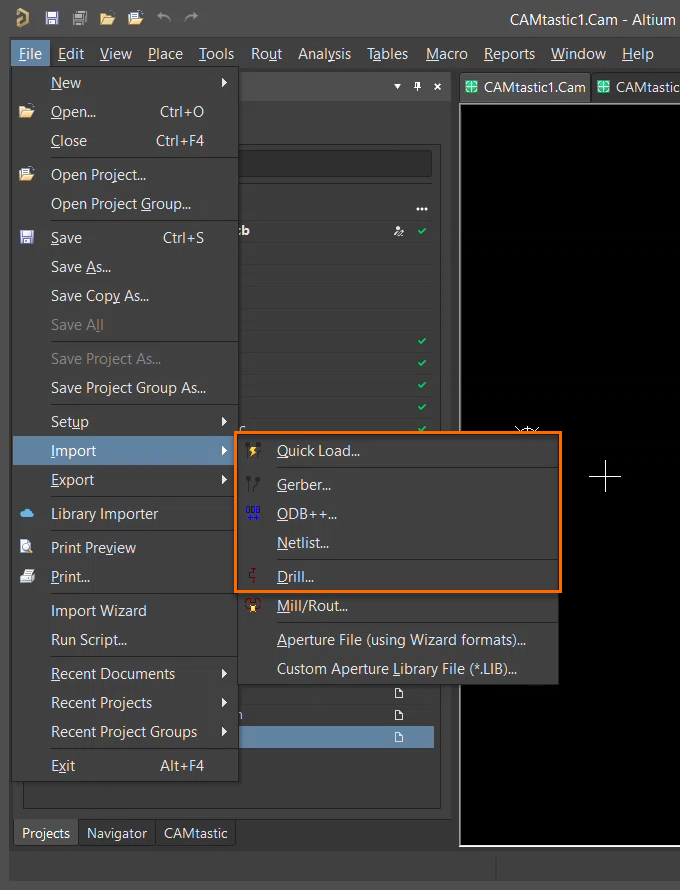
- For a Gerber-based workflow, select File » Import » Gerber... to import the Gerber files.
- For a Gerber-based workflow, select File » Import » Drill... to import the associated NC Drill files.
- For an ODB++ workflow, select File » Import » ODB++... and select the ODB++ root folder.
- If importing Gerber and NC Drill files, import the IPC-D-356 netlist when available using File » Import » Netlist....
- When importing ODB++ data, only import an IPC-D-356 netlist if the required net information is not already included in the ODB++ dataset.
- If all manufacturing files are located in a single folder, File » Import » Quick Load... may be used as an alternative import method.
- Quick Load can import Gerber, ODB++, IPC-D-356 netlists, aperture files, and related CAM data from a single directory.
-
Review import settings if the data does not align correctly.
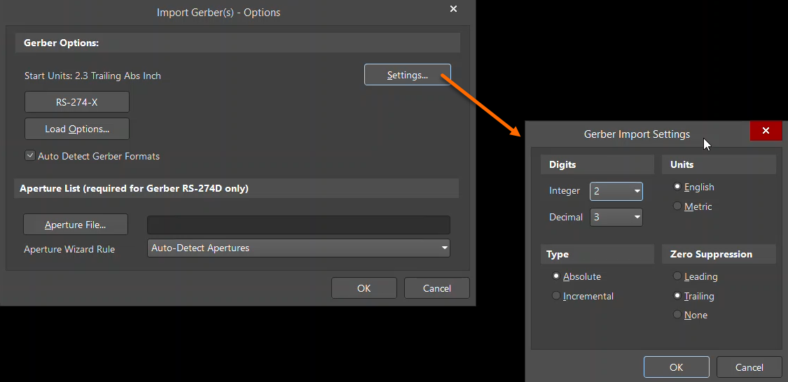
- If imported Gerber data appears incorrectly scaled or positioned, review the Gerber import settings in the CAM Editor Import/Export preferences.
- Verify that the coordinate format and units match the originating CAD system or the information provided with the manufacturing package.
- If Gerber files do not include embedded apertures, import the corresponding aperture file as required.
Gerber Import Settings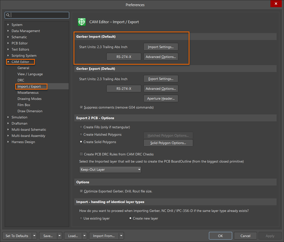
CAM Editor Import/Export Preferences -
Assign and verify layer types.
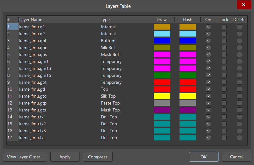
- Open Tables » Layers....
- Verify that every imported layer is assigned to the correct layer type.
- CAMtastic attempts to assign layer types automatically based on layer type detection rules and configured file extensions.
- Open Tables » Layer Type Detection... if the automatic layer assignment needs to be reviewed or adjusted.
- File-extension mappings and Layer Type Detection serve different purposes. File-extension mappings determine whether CAMtastic recognizes a file type during import. Layer Type Detection determines how successfully imported files are assigned to PCB layer types such as Top Layer, Bottom Layer, Internal Plane, Border, Drill, or Temporary.
- If a file does not appear during import, review the file-extension mappings in the CAM Editor miscellaneous preferences. If a file imports successfully but is assigned to the wrong layer type, review the rules in Tables » Layer Type Detection....
- Set mechanical layers to Temporary.
- ODB++ data does not rely on the Layer Type Detection template in the same way because layer identification is stored in the ODB++ matrix file. However, always review the resulting layer assignments after import.
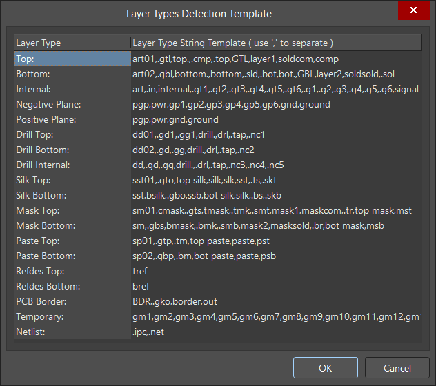
Layers Table Layer Types Detection Template -
Configure the board stackup.
- Open Tables » Layers Order....
- Confirm that the logical and physical layer order matches the actual board stackup.
- Ensure that the physical layer order is valid and that the same order number is not assigned to more than one layer.
- The physical order should place layer number one at the top of the PCB stackup.
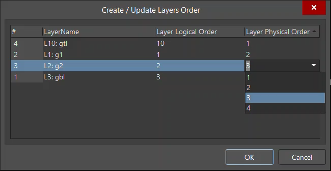
-
Configure drill sets.
- Open Tables » Layers Sets....
- For through-hole-only boards, a single through-hole drill set may be sufficient.
- For boards containing blind or buried vias, create and configure each drill span individually.
- Associate each drill set with the appropriate NC Drill file.
- For blind and buried drill layers, include all layers that are drilled in the layer set, not only the outermost start and stop layers.
- For through-hole drill layers, the start and end layers should usually be sufficient.
- Hold CTRL while selecting the start and stop layers for a drill pair.
- Verify that each intended drill span appears correctly in the Layers Sets table.
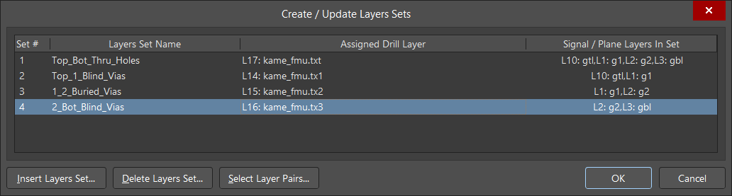
-
Extract the netlist.
- Run Tools » Netlist » Extract.
- The extraction process traces connectivity based on the configured layer stack and drill sets.
- Netlist extraction requires layer type assignments for all layers in the board. Mechanical layers should be set to Temporary.
- After extraction, review the Nets tab in the CAMtastic panel to confirm that nets were generated.
- Although ODB++ may already contain net information, extracting and comparing the netlist provides an independent verification of reverse-engineered connectivity prior to exporting the PCB.
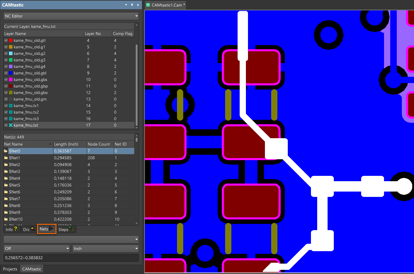
-
Restore net names and compare connectivity when IPC-D-356 data is available.
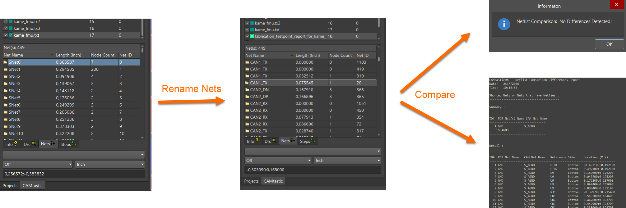
- If an IPC-D-356 netlist was imported, run Tools » Netlist » Rename Nets to restore original net names from the IPC netlist.
- Run Tools » Netlist » Compare to compare the imported IPC-D-356 netlist with the extracted connectivity.
- Netlist comparison provides an additional validation step for through-hole, blind, and buried via connectivity.
- IPC-D-356 netlist data is not required for export, but it is recommended when available because it can restore meaningful net names, help distinguish vias from free pads, and provide a reference for comparison.
-
Prepare the board outline and plane geometry.
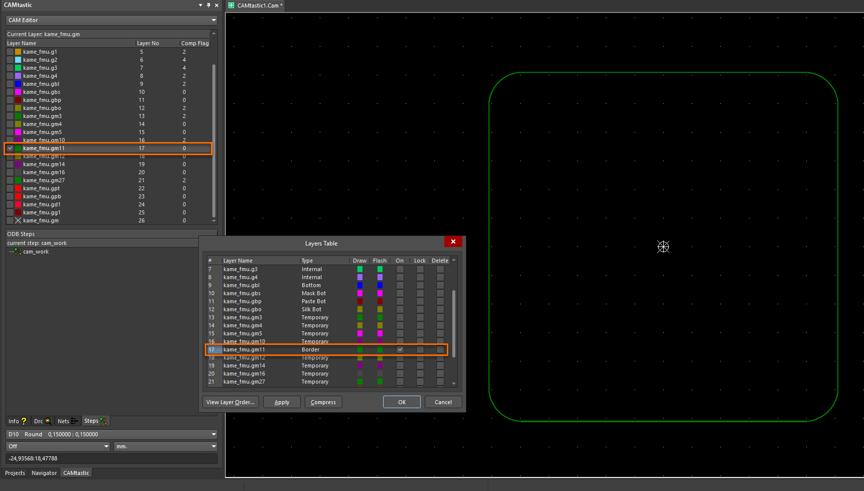
- Before export, ensure a closed polyline exists on a Border-type layer so that a proper board shape can be generated.
- If no closed polyline exists on the Border-type layer, or if multiple layers are designated as Border layers, the generated board shape may not match the intended outline.
- Use Edit » Objects » Join to join outline segments into a closed polyline where appropriate.
- When drawing a new outline, right-click after selecting the final vertex and choose Close.
- All split planes on internal plane layers must be defined by closed polylines.
- Island plane borders may be converted to closed polylines by joining existing segments.
- Split planes that share outlines with other splits or with the board edge may need to be redrawn.
- Nested planes, such as islands inside split planes, are not supported during CAMtastic export and must be corrected manually in the PCB editor after export.
-
Export the reconstructed PCB document.
- After importing fabrication data into a CAM document, the Export to PCB command is expected to be unavailable first.
- The Export to PCB command becomes enabled after a valid netlist has been extracted from the CAM data and the prerequisite layer and drill configuration steps have been completed.
- If the command remains unavailable after completing these steps, review the previous configuration for missing or incorrect data.
- Select File » Export » Export to PCB.
- CAMtastic generates a new PCB document and opens it in the PCB editor.
-
Validate the generated PCB document.
- Verify the board shape, layer stack, drill spans, copper connectivity, split planes, and net assignments.
- As a post-export validation step, verify that NPTH holes have been preserved correctly. In some reported cases, holes identified as NPTH in CAMtastic may appear as plated holes in the generated PCB and may require manual correction.
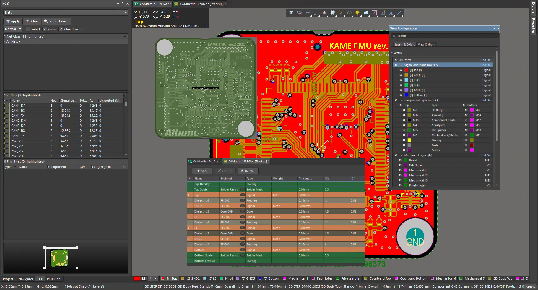
- If not all layers appear at the bottom of the PCB editor after import, open the View Configuration panel using the L shortcut key.
- Right-click in the Mechanical Layers section and add any Mechanical Layer to restore the layer display.
-
Perform post-export cleanup.
- Replace primitive geometry with footprints where required.
- Create PCB library components by copying groups of primitives into a PCB library.
- Replace the original primitive groups with the newly created footprints.
- Redefine drill pairs manually in the Layer Stack Manager if required because drill-pair definitions are not automatically created from CAMtastic Layer Sets.
- Reassign nets to island split planes after export where necessary.
- Exported polygon regions are created as polygon outlines and typically require a repour operation after opening the PCB document.
- Review polygon output and repour polygons if required.
-
Use an alternative workflow for footprint Gerbers if needed.
- Open the footprint Gerber in Altium Designer.
- Select File » Export » DXF.
- Import the DXF into a PCB Library using File » Import » AutoCAD.
- Alternatively, import the DXF into a PCB document using File » Import » DXF/DWG.
Additional Notes
- If the board contains holes or vias, the corresponding NC Drill files are required for accurate reverse engineering. A substitute drill file created from unrelated PCB data will not restore the original drill locations or drill spans.
- CAMtastic can generate a PCB document that closely resembles the original design, but complete reconstruction of the original project may require manual cleanup.
- Pay particular attention to footprints, board outlines, split planes, layer pairs, drill pairs, net assignments, polygon pours, and NPTH hole definitions after export.
- Protel-formatted netlists are not supported for this workflow. The imported netlist must be in standard IPC-D-356 format.