Your Complete Guide to PCB Thermal Analysis

The physical properties of your PCB substrate and copper conductors are the main factors determining how a circuit board will heat up during operation. Circuit board thermal analysis techniques aim to predict when and where a board will heat up during operation, as well as how hot the board will get. This important part of the analysis is geared to ensure component-level and board-level reliability, and it can influence many design decisions.
When you use the best printed circuit board design software, it’s easy to design a board with high reliability and low temperature during operation. Altium Designer has the best circuit board design tools complete with a materials library to help ensure reliability. You’ll have everything you need to implement best practices for thermal management in your PCB layout and your stackup. Here’s how you can better understand circuit board thermal analysis and how to design your next board for reliability.
ALTIUM DESIGNER
A unified PCB design package that integrates advanced layout features with a comprehensive substrate material library and production planning features.
The materials in your circuit board and components will determine how heat moves around the board during operation. Unfortunately, PCB substrate materials are insulators that prevent heat from dissipating away from hot components. Copper conductors and plane layers can help, but there are some simple design choices that will influence the equilibrium temperature of your board as it operates. These design decisions are focused in three areas:
- Circuit board stackup design
- Substrate material selection
- Component selection and layout
In addition to things like electrical fans and heat sinks, some other simple design choices can help ensure your board will run at low temperatures and will not fail prematurely. With the right set of design tools, it’s easy to implement some best practices for thermal management.
Using Thermal Analysis to Design Your Circuit Board
The goal in thermal analysis for circuit board design is to determine when cooling measures like fans, heat sinks, additional copper, or thermal vias are needed to keep the temperature within limits. The designer needs to select the maximum acceptable temperature for components in their board, and then examine how the component temperature will change based on the power it dissipates. If the component temperature gets beyond the acceptable temperature limit, then additional cooling measures like heat sinks or fans may be needed.
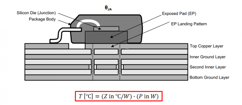
To start, look at the thermal impedance of a component, which is normally found in the component datasheet for integrated circuits. This value can be as low as ~20 °C/W for low-power amplifiers or ICs, or it can be as high as ~200 °C/W for powerful microprocessors. To determine the operating temperature, simply multiply the component’s power consumption by its thermal impedance. This is defined below for an example MOSFET in an SOT package.

Temperature of a component defined in terms of its thermal impedance.
In the event the component’s temperature is too high, there are some steps a designer can take to dissipate heat from the component in order to decrease the thermal impedance of the component in the PCB layout:
- Add thermal vias with grounded polygon pour underneath the component
- Use a PCB substrate material with higher thermal conductivity
- Add a heatsink to the component
- Include more copper below the component, such as a plane layer
- Use a fan to ensure cool air flows across the component package
- Attach the board directly to a metal enclosure with a thermal interface material
No matter which of these routes you take, thermal reliability starts with designing the right PCB stackup using the best PCB design software.
Start With the Best PCB Stackup Design
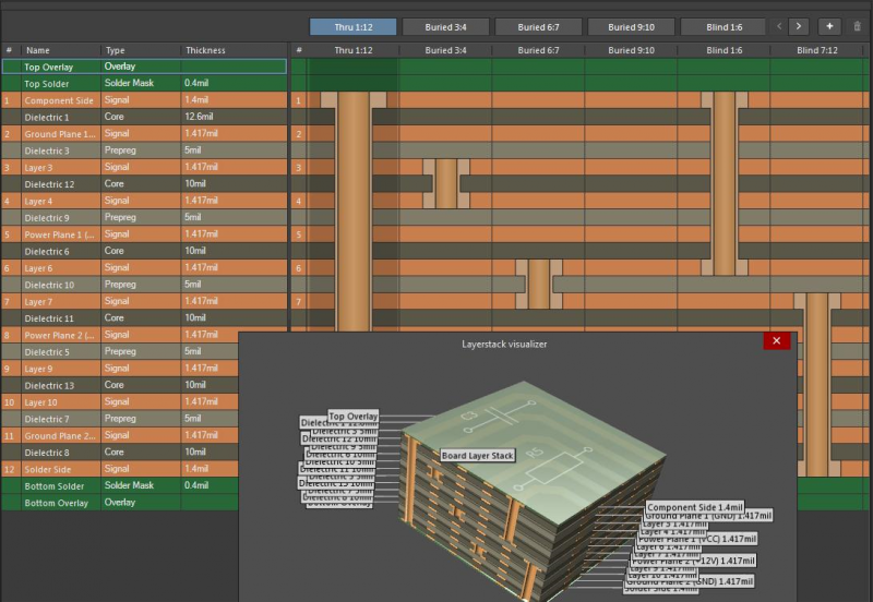
Before implementing any other cooling measures in your circuit board layout, use the best set of PCB design tools to create the correct stackup. Altium Designer’s layer stackup manager lets you create the right arrangement of copper plane layers and layer thicknesses to ensure the PCB substrate has high thermal conductivity. Through-hole vias can be defined in the Layer Stackup Manager to span onto the back of the board beneath hot components. These basic aspects of PCB design go a long way to helping remove heat from hot components.
Altium Designer also allows users to access a PCB stackup materials library with known dielectric properties for common stackup materials. This gives designers full control over their stackup design within their PCB design software, aiding applications like high-speed boards and high current boards for power systems. Design any stackup and select any material for your circuit board in Altium Designer.
- Your substrate material will be a major determinant of reliability. The right material with high thermal conductivity can help remove heat from high-power components and help keep your components running at low temperatures.
- Ceramic materials have much higher thermal conductivity than standard FR4 substrates and are ideal for use in high-temperature environments.
Learn more about designing circuit boards with ceramic substrates.
- No matter which type of materials you want to use for your board substrate, you’ll need the best PCB layer stack manager to create your circuit board stackup.
Learn more about designing your layer stack in Altium Designer.

Stackup design in Altium Designer
Standard Thermal Management Techniques for PCBs
Defining a stackup is just one important aspect of designing your board. Once the stackup is defined in your PCB design software, you can start using your PCB layout tools to place things like ground planes, copper pour, heat sinks, cooling fans, and thermal vias. CAD tools in your PCB layout software are used to define these features in your circuit board. Your PCB libraries should also connect to the electronics supply chain to give you access to CAD models for fans and heatsinks. This makes it easy to find, download, and place the components you need for heat management in your circuit board layout.
In addition to points like placing things like thermal vias, fans, and heat sinks, your plane and trace arrangement on each layer in your PCB will dissipate heat due to the inherent DC resistance of copper conductors in your PCB. When determining how copper should be used in the PCB stackup, DC simulations become important for examining whether hotspots can arise in certain positions in your PDN/
Use DC Power Integrity Simulations to Identify Hotspots
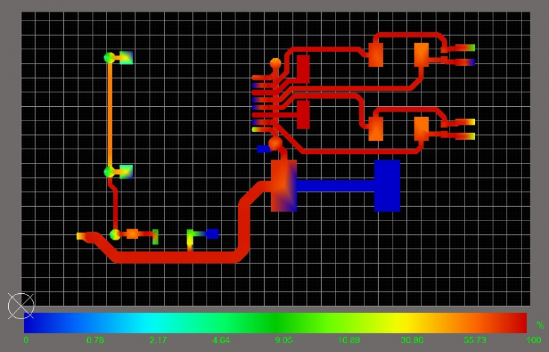
A DC power integrity simulator can be useful for spotting areas in your PDN with high current density, which will then lead to higher temperatures. If these hot regions in the PCB are near a hot component, then some additional copper or heat sink may be needed to help keep the temperature low. In addition, copper in the identified region of the PDN may need to be redesigned to reduce the DC resistance in that region.
- As part of a passive cooling strategy for active components, a thermal pad or thermal paste should be used to bond a heatsink to hot components as this will help efficiently transport heat away from the component.
- Every active component in your PCB acts as a heat source by dissipating some heat in the packaging and in the nearby copper in the PDN. If you have a large number of active components, then you may need to use fans to cool your components.
Learn more about working with active cooling components in your PCB layout.
- The PDN analyzer extension in Altium Designer is easy to access and use. This extension will take your PCB layout data and create high-quality simulations for DC power integrity.
Learn more about Altium Designer’s PDN Analyzer extension for DC simulations.

DC power integrity simulations can help you identify hot spots in a PDN on a single layer or multiple layers simultaneously.
Best Software for Circuit Board Thermal Analysis and PCB Layout
Properly managing heat in your circuit board layout is a difficult task without the right set of PCB layout tools. The best PCB design applications will include more than just a set of CAD tools for PCB layout tasks. You’ll need the best stackup design utility, a comprehensive schematic editor, mixed-signal simulation features, and much more. Once you’re ready to send your board off for manufacturing, you’ll need to create documentation for your design in standard file formats. Your PCB design software should provide all of these features in a single application, rather than separating everything into different programs.
Altium Designer is the only comprehensive PCB design application for any application, ranging from high power DC boards to high-speed digital products and high-frequency RF systems. Altium Designer includes a top-notch layer stackup manager that allows you to import standard materials, define any layer arrangement you can conceive, and import unique materials. You’ll also have access to a complete set of routing and layout features complete with via and polygon design tools. Everything you need to design reliable circuit boards is included in Altium Designer.
Design the Most Reliable Circuit Boards in Altium Designer
The power of Altium Designer lies in its rules-driven design environment. Other design platforms separate your important design tools into different programs, but Altium Designer keeps you productive with a single application. The PCB design features in Altium Designer are built to work together in a single package and will help you spot errors as you create your design. No other PCB design application gives you access to this many features for circuit board thermal analysis, layout, and manufacturing.
- Altium Designer is the ideal package for professional PCB design teams that want a complete set of design tools in a single application.
Learn more about Altium Designer’s unified design environment.
- The PDNA extension for Altium Designer is accessible inside our PCB layout and can help you spot regions of your layout that will be too hot during operation.
- When you need to share your circuit board designs with other PCB designers or your manufacturer, you can instantly share your design and production data through the Altium 365 platform.
Learn more about sharing your PCB project data with Altium 365.

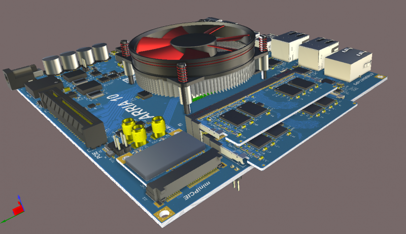
3D view of a multi-board system with a large cooling fan
Once you’ve done your circuit board thermal analysis and identified potential problems in your PCB layout, use Altium Designer to implement best practices for keeping your board’s temperature within limits. No other design application provides a complete set of design, sharing, and design verification features in a single application.
Altium Designer on Altium 365 delivers unprecedented integration to the electronics industry until now relegated to the world of software development, allowing designers to work from home and reach unprecedented levels of efficiency.
We have only scratched the surface of what is possible to do with Altium Designer on Altium 365. You can check the product page for a more in-depth feature description or one of the On-Demand Webinars.


