How to Calculate Impedance-Controlled Routing In Your PCB And Design Rules

Once you start designing high-speed or high-frequency PCBs, impedance in your traces becomes a critical parameter to consider during design. Impedance mismatches between signal sources, loads, and each trace that connects them can ruin a signal. Instead of working out the impedance of each trace in your PCB by hand, Altium Designer aids impedance-controlled routing with an integrated field solver. This streamlines your design process and ensures impedance calculations are accurate throughout your layout.
ALTIUM DESIGNER
A fully unified, heavily rules-driven PCB design platform for impedance controlled routing in high-speed PCB design.
Signal problems can abound when trace width values are incorrectly specified in high-speed PCBs. Reflections, ringing, and overshoot result from traces on the PCB without effective impedance controlling routing. Mismatches occur due to impedance discontinuities, such as changes in trace width, lack of termination, T-stubs or bifurcated traces, vias between routing layers, large power plane discontinuities, and connector transitions.
Rather than reinvent the wheel, your PCB design software should integrate signal integrity tools for ensuring accurate impedance control throughout your layout. Many trace impedance values simply can’t be calculated by hand, and you need methods to ensure each signal reaches its destination without excessive loss or distortion. Altium Designer has the signal integrity tools you need for impedance-controlled routing and many other tasks that are central to high-speed design. Here’s what you need to pay attention to in high-speed design and analysis.
Impedance Controlled Routing Starts with the Right Calculator
In some cases, impedance calculators can be very useful as they allow you to calculate the impedance of an isolated trace by determining the perfect width to prevent signal reflections. The equations that define the impedance in a trace are specific to the geometry of the trace, and they assume the trace is isolated from any other trace on the board. In a real PCB, this is not the case as traces couple to each other capacitively and inductively. The strength of any coupling affects the impedance seen by groups of signals and is influenced by the dielectric constant of the substrate.
It’s not that trace impedance calculators are inaccurate, but rather that they have limitations as far as their applicability. For example, the equation for the trace impedance in a differential pair of asymmetric striplines includes an approximation on the dielectric constant and geometry. Other calculators will use different equations for the same system, depending on the relevant approximations used in the derivation of the formula. Most calculators will allow you to place invalid values that fall outside the approximation range for common trace geometries (microstrip vs. stripline), which then produce inaccurate results.
Getting the Most Accurate Impedance Calculations
Tuning for your traces to the desired impedance value occurs by adjusting trace width and distance from the reference plane. Ensuring impedance-controlled routing also requires knowledge of the substrate’s dielectric constant and your required trace width. The most accurate way to account for both characteristics in your board simultaneously is to use an impedance calculator with an integrated field solver. This will aid your other design and signal analysis tools as you route each trace and create your PCB layout.
- If you’re not familiar with signal integrity problems that can arise from impedance mismatches, there are some basic steps you should take with your signal integrity tools in high-speed design.
Learn more about the basics of signal integrity analysis in your PCB.
- Trace impedance calculators can help you determine the right trace width for your board. You’ll need to know the dielectric constant of your substrate at the relevant frequency and some parameters in your layer stackup.
Learn more about using trace impedance formulas and calculators.
- Your layer stack will affect your trace impedance, and this should be accounted for when defining design rules and routing traces.

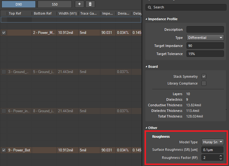
Defining a differential impedance controlled routing profile in Altium Designer
Impedance Calculations in Your Design Rules
Your design rules are built to ensure your printed circuit board will function as intended. If you’re unsure of how best to route traces between components, where to place components with respect to ground/power planes, or whether you’ve properly designed your pads and vias, your design rules are there to keep you in check.
Your design rules are also meant for more than just checking component placement. Certain features in your layout like trace width, trace length, and vias have important rules and constraints on their geometries and spacing that should be followed. This is all meant to maintain signal integrity and ensure your board can be reliably manufactured. If your PCB design software has a powerful rules-checking engine, you can prevent signal integrity and ensure your device works properly as soon as it leaves the production line.
EDA tools contain calculators for determining propagation delay, appropriate trace length, and trace impedance. If you’re using a PCB design application with an integrated field solver, you can examine all of these aspects of PCB design as you create your layout. The same field solver will examine all these aspects of your layout as you route copper traces across any layer in your board. You can then visually see when your traces have the correct impedance and propagation delay, both of which you can easily define in your PCB design rules.

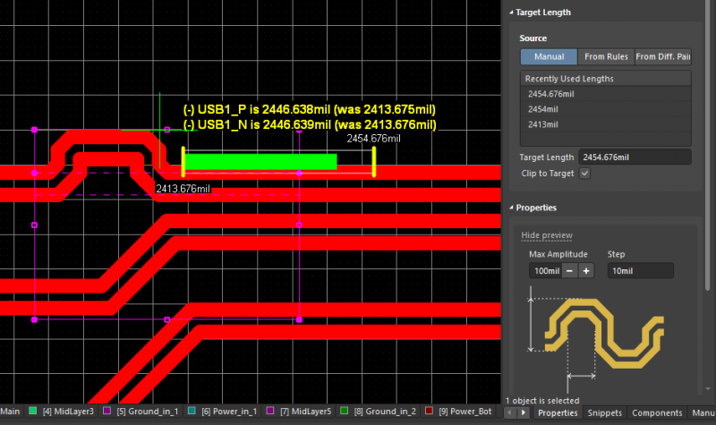
Examining trace length matching for differential pairs in Altium Designer.
Ensure Your Layout Complies with Your Design Constraints
Ensuring your layout complies with the relevant constraints for your application requires defining design rules for your new board. This not only aids important tasks like ensuring consistent trace widths and lengths in each layer, but it also ensures consistent impedance throughout your printed circuit board. A powerful rules editor is one of the first features you’ll access when you create your circuit board schematics, but it will help ensure your board operates correctly and is manufacturable at scale.
- Your PCB software should make it easy to work with high-speed design rules and constraints within a single interface.
- When working with differential pairs, your trace spacing and geometry will determine the impedance of each trace and of the pair. This is one of many parameters you can specify in your design rules.
Learn more about design rules for trace width and spacing while routing your layout.
- Impedance-controlled routing sometimes requires terminating traces at different components, such as when routing LVDS. Your PCB software should be adaptable and allow you to apply any termination method.
Learn more about termination methods for your high-speed/high-frequency PCBs.

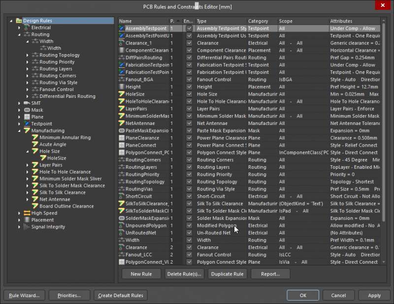
The design rules editor in Altium Designer
The Most Advanced Models for Impedance Control
Getting impedance calculations extremely accurate requires accounting for dispersion in the substrate’s dielectric constant and the complex geometry of a typical PCB trace. An online calculator simply won’t do the trick. You can do some calculations by hand, but the easiest easy to ensure consistent impedance in your board is to use routing tools with an integrated field solver. This allows you to design impedance-controlled traces with any width and arrangement in your PCB.
Advanced modeling tools for PCB traces require an accurate model for dispersion in the dielectric constant. These features also need to integrate with your design rules in your PCB design software to create a productive design environment. This is the type of environment you’ll find in Altium Designer, the world’s only fully integrated platform for printed circuit board design.
The Unified Design Environment in Altium Designer
Altium Designer places rules checking, signal integrity, and DFM at the core of the design process. All the signal analysis and design verification tools are built to work together with your CAD features and routing tools. The rest of the PCB design industry still segregates these features into different programs with different workflows. Instead of working under the same old paradigm, it’s time to take the plunge into unified design.
- A rules-driven design engine is at the core of Altium Designer. This unique software architecture allows your signal integrity tools and field solver to quickly verify every aspect of your layout as you create your circuit board.
Learn more about the rules-driven design engine in Altium Designer.
- When you need to design your trace geometries with consistent impedance, you can use the integrated field solver in Altium Designer. This tool includes copper roughness in calculations for most common trace geometries.
Learn more about Simberian’s integrated field solver in Altium Designer.
- Consistent impedance-controlled routing requires customizing your board with a layer stack manager. Altium Designer includes the best layer stack manager for designing trace width and impedance in your printed circuit board.
Learn more about Altium Designer’s advanced layer stack manager.
The unified design environment in Altium Designer brings all your design features together into a single interface. These tools are designed to work together as part of a single platform for any application, including advanced high-speed boards and HDI designs. If you want to calculate the perfect trace width and impedance, Altium Designer has the tools you need for success.
Altium Designer on Altium 365 delivers an unprecedented amount of integration to the electronics industry until now relegated to the world of software development, allowing designers to work from home and reach unprecedented levels of efficiency.
We have only scratched the surface of what is possible to do with Altium Designer on Altium 365. You can check the product page for a more in-depth feature description or one of the On-Demand Webinars.


