Photodiode Circuit Simulation and Design for Your PCB

Table of Contents
Your design tools should give you an easy way to create circuit diagrams, simulate electrical behavior, and start a new PCB layout. A photodiode circuit is important in many applications, ranging from simple ON/OFF light detection to receiving digital data in an optical fiber. These semiconductor devices are similar to a regular diode, but they can be difficult to simulate without the right component models and circuit design tools.
With Altium Designer, you won’t need to use separate applications to create your photodiode circuits, run simulations, and prepare your PCB layout. Everything happens within the same application, helping you stay productive. If you’ve never designed a photodiode circuit and you need tools to get the job done, here’s how Altium Designer can help you.
ALTIUM DESIGNER®
The industry’s only design application that offers full customization of your PCB project data and design libraries with a complete set of PCB data management tools.
Photodiodes are a simple but important circuit element in opto-electronic systems. These designs need to convert light into an electrical signal for a range of applications. Ideal applications range from simple DC light detectors with thresholding (ON-OFF detection) to pulse detector circuits for lidar systems. No matter how you want to use a photodiode, you’ll need to design a photodiode circuit and simulation before you create your PCB layout.
Designing a Photodiode Circuit
A photodiode is a simple photosensitive device that converts light into electricity. A photodiode can also be placed in a reverse biased circuit so that it produces a small amount of current when not illuminated. The goal in using a photodiode circuit is to collect and amplify the reverse bias current produced from the photodiode once it is illuminated. The output current will be a linear function of input optical power:

Current produced in a photodiode
From the above equation, the output current scales relatively linearly at low reverse bias. When designing a photodiode circuit, the goal is to collect the current and convert it to a useful signal level with an amplifier. The gain in the amplifier stage needs to be matched to the ADC input, but the gain also needs to be large enough to sufficiently amplify the photodiode output. In addition, the gain in the photodiode circuit should not be so large that the circuit becomes saturated.
Finding and Selecting Photodiodes in Altium Designer
There are many important parameters to consider when selecting a photodiode. Among these are:
- Responsivity spectrum and sensitivity
- Temperature coefficient
- Reverse bias saturation current
- Whether an avalanche photodiode should be used
- Parasitics (capacitance and shunt resistance)
Building a photodiode circuit requires finding the right parts, including component models and SPICE simulation circuits for your circuit and components. When building a simulation of a photodiode circuit, each of these aspects needs to be included in the simulation model to ensure the electrical behavior of the circuit can be accurately described. For simulation, schematic design, and PCB layout, you’ll need sourcing tools that integrate with your component libraries to ensure you can build accurate photodiode circuits and simulations.
Altium Designer integrates with the larger electronics supply chain through the Manufacturer Part Search panel, giving you complete visibility into the electronics supply chain. Designers can pick the appropriate photodiode, see sourcing data and pricing, and spot components with verified footprints.
- Use the Manufacturer Part Search panel in Altium Designer to find component models and simulation models for your components. You’ll need to use accurate component models for your schematics to create your photodiode circuit.
Learn more about the Manufacturer Part Search panel in Altium Designer.
- An important part of designing a photodiode circuit is the amplifier stage, which increases the output signal from the amplifier so that it can be measured with an ADC.
Learn more about creating an amplifier simulation in Altium Designer.
- High precision opto-electronic systems need low skew, low parasitics, and stable power to operate properly.
Learn more about working with high precision opto-electronic components in your PCB.

Find the photodiode circuit components you need with the Manufacturer Part Search panel in Altium Designer.
Photodiode Circuit Simulations
Photodiode circuit simulations aim to examine some of the following electrical behavior:
- Transient response to input light pulses or continuous light
- Using a load line to determine photoconductive vs. photovoltaic mode
- Determining the responsivity
- Determining changes in electrical behavior vs. temperature changes
- Designing the correct level of gain into the amplifier stage
Some of these aspects require using an accurate component model for a photodiode, but others require using simulation sources to model input light and the effects of placing the circuit in reverse bias. SPICE simulators can be used as long as the components you select include accurate SPICE subcircuits for mixed-signal simulations.
Building Accurate Simulations in Altium Designer
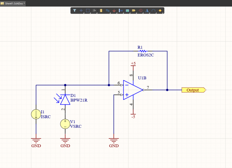
The generic components in Altium Designer and the Simulation Sources library can be used alongside manufacturer-provided simulation models and custom SPICE subcircuits. For a photodiode circuit, a simulation model involving a biased photodiode and a current source will be used to simulate an illuminated photodiode. Altium Designer’s component tools and schematic editor make it easy to build simulations for your photodiode circuit.
The MixedSim tool in Altium Designer is designed to enable logic-level simulations, analog simulations, and DC simulations. Designers can build models for their photodiode circuits using commercially available components and generic components. They can also perform all of the standard simulation tasks one would find in a SPICE package, but in a user-friendly interface with intuitive visualizations. Best of all, these simulation tools are available in the same application as your schematic editor and component selection tools.
- Your photodiode circuit simulation will start with the right SPICE package. Altium Designer includes a proprietary SPICE solver alongside standard ECAD tools.
Learn more about SPICE simulations in your PCB design software.
- Altium Designer circuit design and PCB layout features are ideal for creating an amplifier stage to support your photodiode circuit.
Learn more about designing an amplifier schematic and PCB layout in Altium Designer.
- Altium Designer’s schematic editor enables hierarchical design so that multiple circuit blocks can be cascaded together into a larger system. It’s easy to keep your schematics organized in Altium Designer.
Learn more about organizing your schematics in Altium Designer.

Building a simulation model for a photodiode circuit.
Schematic Design, Simulation, and Layout in One Application
With the complete set of circuit design and simulation features in Altium Designer, you’ll have a complete set of tools for creating and simulating photodiode circuits. You can do much more than run simulations and determine load lines. Altium Designer’s unified rules-driven design engine ensures all your design tools are integrated into a single program and will work together with the same set of design rules. In addition, the component management tools let you assign the simulation models you need for your components to properly simulate your photodiode circuits.
Altium Designer and Altium 365 Unify PCB Design and Management
With the Altium 365 platform, designers can share their Altium PCB projects with remote collaborators in a secure cloud platform. When your team uses the Altium 365 platform, they can easily access and collaborate on circuit board design projects within Altium Designer. It’s never been easier to share schematics, components, simulation models, PCB layout files, and manufacturing packages.
- Altium Designer is the only design platform that unifies a complete set of powerful design and simulation features in a single program. You can design a photodiode circuit or any other circuit you can imagine in Altium Designer.
Learn more about printed circuit board design in Altium Designer’s unified environment.
- Because everything you need for design is in one place, it’s easy to build simulations from your circuit schematics. You can then use schematic capture to import your components into a PCB layout in a single application.
Learn more about the complete set of design tools and processes in Altium Designer.
- When you’re ready to share your photodiode circuit designs and manage your data, you can use the Altium 365 platform. Store and share all designs, simulation models, and PCB projects in a single cloud-based platform.

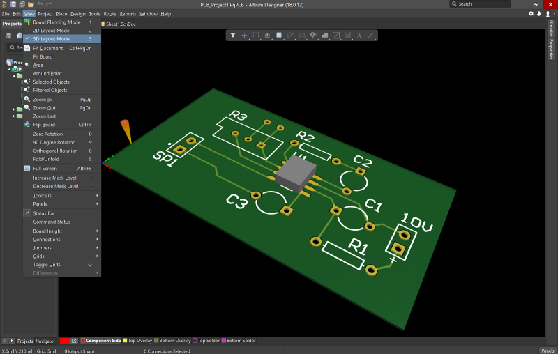
Altium Designer’s complete set of PCB design tools can help you create your photodiode circuit schematics and PCB layout.
Altium Designer is the only unified PCB design platform for designing and simulating circuits of any complexity, and for creating high-quality PCB layouts with a powerful set of CAD tools. With the Altium 365 platform, your team can operate with maximum efficiency in Altium Designer’s integrated environment. Make the switch today to get access to the industry’s best circuit board design tools and data management features.
Altium Designer on Altium 365 delivers unprecedented integration to the electronics industry until now relegated to the world of software development, allowing designers to work from home and reach unprecedented levels of efficiency.
We have only scratched the surface of what is possible to do with Altium Designer on Altium 365. You can check the product page for a more in-depth feature description or one of the On-Demand Webinars.


