Power Delivery Systems Design

Table of Contents
This article is intended to define the new challenges and provide guidance in how to successfully engineer the Power Delivery System (PDS) so it meets the needs of new technologies.
As integrated circuit technology allows for billions of transistors on a single IC, it has resulted in very powerful systems on a chip. This has made it possible to put the equivalent of supercomputers inside video games, cell phones, and a host of other products that once occupied entire computer rooms. This same IC technology has made it possible to create output signals that are in the multi-gigahertz range, once only possible with very expensive microwave circuits. All this technology needs a great power delivery system design behind it.
As with most advances of this nature, there are side effects that need to be addressed. These very large ICs often need several different operating voltages, most of which are not much higher than 1 volt with currents that can reach over one hundred amperes. Along with this, as will be seen later, the frequencies demanded from the power delivery rails of a PCB can extend as high as a gigahertz. Meeting all these requirements is a complex task that forces designers to use much more engineering skill than was needed by previous levels of technology. Unfortunately, most of the methods currently in applications’ notes do not offer the advice that is needed. This chapter is intended to define these new challenges and provide guidance in how to successfully engineer the Power Delivery System (PDS) so it meets the needs of these new technologies.
AN IDEAL POWER SUPPLY
Figure 5.1 depicts an ideal power supply. An ideal power supply is often called a voltage source. Power delivery system voltage sources have zero output impedance so that no matter how much load (current) is demanded of the power supply the output voltage remains constant. That means as little as possible between the USB power plug and power draw point. Further, no matter at what frequency the current is demanded the output voltage remains constant. Unfortunately, real power supplies are not like this. They all have an output impedance that is not zero either at DC, or at frequencies needed by modern logic.
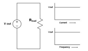
Figure 5.1 An Ideal Power Supply
A REAL POWER SUPPLY
Figure 5.2 depicts a real power supply. As can be seen, there is an output impedance in series with the voltage source. This diagram illustrates the power delivery system design problem.
This power delivery output impedance varies with frequency, resulting in high impedances at some frequencies and low impedance at others. Where the output impedance is high, changes in demand for current will result in changes in output voltage. This is what is known as ripple. The designer’s goal is to design a PDS that has an output impedance that is low at every frequency where the loads require current in order to minimize ripple.
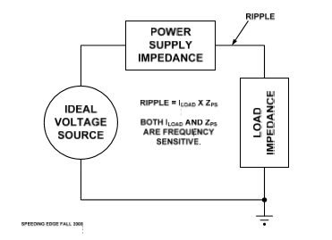
Figure 5.2 A Real Power Supply
WHAT IS RIPPLE?
Ripple is a voltage variation on the Vdd rail of a power supply. Ripple is the result of changes in load current developing a voltage drop across the output impedance of the supply, thus reducing the supply voltage seen by the load. Excessive ripple can cause a system to malfunction by making the Vdd voltage too low for the circuit it powers to operate correctly. Excessive ripple has been shown to be the primary source of EMI in most systems. It couples directly onto signal lines routed over the Vdd planes in a PCB. (This is what gives rise to one of the rules of thumb that “critical” signals must route only over the ground planes.) Excess ripple is often the reason given for using only linear supplies to power the SERDES (serializer/deserializer) in high-speed links.
There is often confusion about where ripple comes from. It isn’t some “noise” that comes from some mysterious source that must be “bypassed” or “decoupled.” If there is ripple on a voltage rail it is a red flag that the impedance of the PDS is too high at the frequencies contained in the ripple. The remedy is to redesign the PDS to reduce the impedance at those frequencies. The usual method for reducing the impedance of the PDS is to add “decoupling” capacitors. Again, they are not decoupling anything. They are providing a local source of charge to support a switching event. A better name for them is “coulomb buckets” as they store coulombs of charge used to support switching events. Once this is understood, figuring out how many coulombs at what frequencies are needed in the PDS is the engineering task.
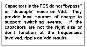

Ripple on Vdd
CAPACITORS OR COULOMB BUCKETS
Every designer has been asked to place capacitors around logic and analog components. In most cases, the instructions as to how many and where they must be placed are taken from an applications’ note. It is rare, if ever, that these applications’ notes have been engineered to assure that the right kind and quantity of capacitors are being used, or that their location is well defined.
It is important to recognize that capacitors have two parasitics that limit their ability to provide charge to switching events on a PCB. Figure 5.3 is a diagram of an ideal capacitor, a real capacitor, and the impedance vs. frequency of the real capacitor. Notice that the real capacitor has an inductance (Lp) and a resistance (RP) in series with it. These are unwanted parasitics that are an unavoidable part of every capacitor no matter how small.
At the bottom of Figure 5.3 are two equations. These allow calculation of the impedance of the L and C as a function of frequency. Notice that at DC or f = 0, the impedance of the capacitor is infinity and it is not visible to the PDS loads. Notice that at DC or f = 0, the impedance of the inductor is zero and it is not visible to the PDS loads. As f goes up, Xc goes down and XL goes up. At one and only one frequency, Fr. These two impedances are equal and cancel each other, and the impedance that is seen by the PDS loads is the parasitic resistance R. It is at this frequency that the coulomb bucket is most useful in the PDS.
Below Fr, the capacitor becomes a high impedance and cannot supply charge to a load. Much above Fr, the capacitor begins to look like an inductor that is in parallel with the plane capacitance of the PCB forming a parallel-tuned circuit. This parallel-tuned circuit can create an impedance high that will result in very high ripple voltages at the resonant frequency of the parallel-tuned circuit.
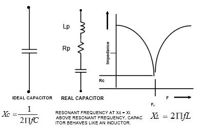
Figure 5.3 Ideal and Real Capacitors
IMPEDANCE vs. FREQUENCY OF A PDS
When designing a PDS, the task is to create a low impedance across a wide range of frequencies. Figure 5.4 is the impedance vs frequency of a single 0.1 uF and a single 0.01 uF capacitor when mounted between Vdd and Vss of a set of power rails. The blue curve is the impedance profile of the 0.1 uF capacitor, the yellow curve is the impedance of the 0.01 uF capacitor, and the red curve is the impedance of these two capacitors combined.
Most applications’ notes instruct the designer to place some number of these two values of capacitors on each power rail. What can be seen from Figure 5.4 is that the impedance is lowered to 100 milliohms between 6 MHz and 15 MHz. On either side of this range, the impedance increases rapidly. Imagine that there is a delta I of 1 ampere at 100 Mhz. The ripple at this frequency would be 500 millivolts. At frequencies above this, things would get even worse.

Figure 5.4 Impedance vs Frequency of a .01 uF and a 0.1 uF Capacitor on a PDS
WHAT LOADS LOOK LIKE
A good question to ask is what do the loads look like that the PDS must support. In most CMOS-based systems the transmission lines are series terminated as shown in Figure 1.7 in Chapter 1 of this book. The voltage waveform when such a circuit switches from a 1 to a 0 and back again is shown in Figure 1.12. Current will be drawn from the PDS to charge up the transmission line. In order to determine what the frequencies are in that current waveform it is necessary to do a Fourier transform. Figure 5.5 shows the current waveform at the top in red. The positive going excursion is current drawn from the PDS to charge up the transmission line as it goes from a logic 0 to a logic 1. The negative going excursion is the current waveform as the charge is being removed from the transmission line, as it goes from a logic 1 to a logic 0.
The lower part of Figure 5.5 is a Fourier transform of the current waveform that charges the transmission line from a logic 0 to a logic 1. This shows the frequencies needed from the PDS to create a proper logic waveform. In this example, the transmission line is 12 inches (30 cm) long and the clock frequency is 30 MHz. Notice that there are frequency components that start around 80 MHz and range up to about 900 MHz. None of these are harmonics of the clock. The highest frequency is set by the rise time of the switching edge (1 nSec) and the lowest frequency is set by the length of the transmission line.
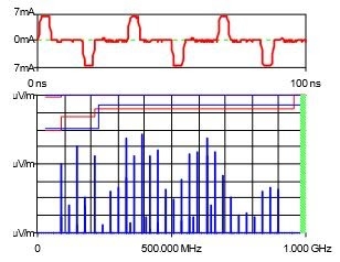
Figure 5.5 Fourier Transform of Current Waveform Driving a Series-Terminated Transmission Line
Referring back to figure 5.4 it can be seen that the classic 0.1 uF, 0.01 uF capacitor strategy recommended by so many application notes only deals with frequencies up to about 30 MHz. None of the frequency components are not supported by the PDS and appear as ripple noise on Vdd. This noise will couple onto any signal routed over the Vdd plane, and can escape the PCB on signal cables. This is the primary source of EMI in nearly all systems that fail EMI. This same noise appears on any logic signal that is at a logic 1 because CMOS shorts signal lines to Vdd when at a logic 1.

Primary source of EMI
In 1995 this fact was demonstrated by the EMC faculty of the University of Missouri, Rolla, now known as the Missouri University of Science and Technology. To demonstrate the problem and how to solve it, a study was conducted to see what happens when the classic approach to bypassing the PDS is used, and how to solve the problem. Item 1 in the references at the end of this chapter is the result of that study. Anyone designing A PDS is encouraged to read this study. Figure 5.6 is an impedance vs. frequency plot of the test PCB used in the study. The test PCB had a plane capacitor of about 15 nF.
There are three impedance vs. frequency curves in Figure 5.6. The first is the impedance of the bare PCB showing only the impedance of the plane capacitor. The second is the impedance of the board with one .1 uF and one .01 uF capacitor added and the third is with one 0.1 uF capacitor, and four .01 uF capacitors. As should be expected, when only the bare board is tested, the impedance is very high at low frequencies because the size of the plane capacitor is small. In the second curve, when two capacitors are added as might happen by following an applications note, the combined impedance is low where the .1 uF capacitor is series resonant (about 13 MHz), and increases as the frequency goes up and drops again as the .01 uF capacitors becomes series resonant (about 45 MHz). Between 50 MHz and 100 MHz, the impedance is worse than if no capacitors were added. This phenomenon is often referred to as an impedance “hole”. It is the result of the parasitic inductance of the .01uF capacitor and its mounting inductance forming a parallel-tuned circuit with the plane capacitor of the PCB.

5.6 PDS Impedance vs. Frequency Plot from UMR Study, Plot courtesy of the IEEE
A solution to this problem that is often proposed is to add more capacitors. The third curve is the result of adding more .01 uF capacitors, in this case 4. The only thing that has changed is that the impedance low created by the .01 uF capacitors is much lower and has moved up slightly in frequency and the impedance hole has moved up in frequency but is still there. How to make this impedance “hole” go away will be discussed later in this chapter. Notice that above about 140 MHz, there is no change.
Unlike the impedance profile in Figure 5.4 the impedance above 100 MHz is relatively low. The reason for this is the presence of the plane capacitor. It is this capacitor that supports the frequencies in the switching waveform above 100 MHz. It was the purpose of the UMR paper to show EMI engineers that successful containment of EMI depended on engineering a good plane capacitor on each rail that supports switching waveforms.
Most modern processors have standby and active modes to minimize power consumption when there is little or no activity. This is especially important when a product is battery powered such as a cell phone. When these processors go from standby to active, a current transient similar to that shown in Figure 5.5 results. Handling these current transients is done using the same techniques used for switching transmission lines.
PLANE CAPACITANCE
It has been demonstrated above, and in many other places, that a plane capacitor is necessary for proper operation of most power delivery systems. This is achieved by separating the Vdd and Vss planes by very thin dielectrics. Figure 5.7 is a plot of capacitance per square inch as a function of separation between the planes for a dielectric constant of 4, which is typical of most laminates used for this purpose. There are two curves plotted, one red and one black. The red curve is the capacitance per square inch for planes that are solid and the black curve is the capacitance per square inch when there is a high concentration of holes in the planes caused by densely packed components such as BGAs.

Figure 5.7 Capacitance per Square Inch for Two Parallel Planes as a Function of Separation
DETERMINING THE AMOUNT OF PLANE CAPACITANCE NEEDED
Determining how much plane capacitance is needed for a given power rail is a complex analysis. An engineer needs to employ one of the tools listed later in this chapter to do this. This analysis involves a simulation that includes a variable current load and a variable plane capacitor. The load is switched off and on, and the amount of ripple is measured as the size of the plane capacitor is increased. Once the ripple target has been reached, the size of the plane capacitor has been determined. At this point, it is possible to design the PCB stackup to include enough plane capacitance for each power rail.

PDS design precedes PCB stackup
CREATING PLANE CAPACITANCE
It is clear that almost all power rails in modern PCBs require some plane capacitance to support the fast switching edges contained in logic signals. The question that arises is how to create such plane capacitors. Figure 3.9 in Chapter 3 shows a 10-layer PCB with two closely-spaced plane pairs, Layers 3 & 4 and Layers 7 & 8. These are separated by only 3 mils (75 microns) to create interplane capacitance.
What if the usual layer stackup that has worked in the past does not have enough plane pairs to create the needed capacitance? There are two solutions. Choosing not to create a stackup that has the required plane capacitance is not one of them. The easiest choice is to add additional plane pairs to solve the problem. For a number of reasons, this may not be an option.
Figure 5.8 illustrates how this problem was solved with a 6-layer PCMCIA PCB that could not accommodate an additional pair of layers for both cost and thickness reasons. This design failed EMI tests six times. Each time the engineers changed the population of the discrete capacitors hoping to fix the problem with no luck. The reason this did not work is well articulated in the UMR paper cited above. An 8-layer version of this design was fabricated adding two power layers to create a power plane capacitor and the EMI problem went away. There were two problems with this solution. One is the PCB was too thick to fit in its enclosure, and the other is that the added cost of the two additional layers made the product uncompetitive in the market.
On layers 1, 3, 4 & 6 copper is represented in black. On layers 2 and 5, the original power and ground layers, the copper is shown as white.
On inspection of the four signal layers, 1, 3, 4 & 6 it was clear that there was substantial unused space on them that could be filled with copper and create plane capacitance. When this was done, the plane capacitance before the fill was done, was half a nanoFarad, and the after capacitance was four nanoFarads, enough to solve the EMI problem.
Figure 5.8 shows the stackup of this PCMCIA PCB before filling these signal layers on the left and after on the right. As can be seen from the figure, the before stackup had only one plane capacitor with a 12-mil separation, and the after has five plane capacitors with 4-mil separations.
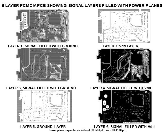
Figure 5.8 A 6 Layer PCMCIA Card Showing Signal Layer Fill to add Plane Capacitance

Figure 5.9 Before and After Six Layer Stackup of PCMCIA PCB
LOCATION OF CAPACITORS
Most designers have seen a wide variety of “philosophies” for locating bypass capacitors, also known as decoupling capacitors. Some of them are listed below.
- As close as possible to each power lead
- By every power lead
- Under the component
- Use traces to connect the capacitor to each power lead.
None of these seem very precise. There must be a precise method for determining the location of capacitors that ensures they do their job properly and, at the same time, makes layout and assembly as easy as possible. In fact, there is a well-defined method that has been in use for a very long time in companies that have been designing high-performance products. It is understood by these companies that plane capacitance is a necessary component of a PDS. When this plane capacitor is part of the PDS, the inductance of the plane pair is several orders of magnitude less than the mounting inductance of each capacitor.
Figure 5.10 is a test PCB with well-engineered plane capacitance in it. This test PCB was used to make a wide variety of measurements concerning how capacitors behave. In this example the question being asked is if an IC were mounted in the upper left corner of the PCB, could it detect whether a capacitor was mounted at C1, C2, C3, or C4? This test will determine where a designer needs to place each capacitor to achieve the best performance.
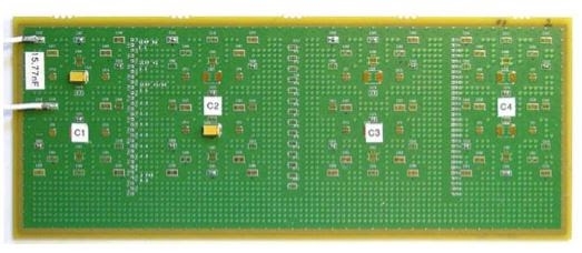
Figure 5.10 Test PCB Used to Evaluate Location of Capacitors
Figure 5.11 is the measured impedance vs frequency of the four capacitor locations. Notice that the four curves are virtually identical indicating that the location of the capacitor made very little difference in the overall impedance of the PDS. The little difference that is seen is the result of the spreading inductance of the plane pair as the capacitor is moved farther from the IC. It should be noted that C1 is about ½ inch (1.25 cm) from the IC and C4 is about 9 inches (23 cm)!

Figure 5.11 Impedance vs Frequency of Four Capacitor Locations in Figure 5.8
The conclusion that must be drawn from the above tests is that location of bypass capacitors in PDS designs that include a plane capacitor is of very little importance. The author’s instructions to a PCB designer is to place the capacitors where they don’t interfere with layout and make assembly as easy as possible. All the application notes that insist on cramming capacitors between the vias under a BGA or “as close as possible” are making design and assembly difficult and more expensive for no good reason.
Figure 5.12 is an example of a PCB designed with the bypass capacitors placed where they do not interfere with layout.

Figure 5.12 A PCB Design with Well Placed Capacitors

Bypass capacitor tip
MINIMIZING IMPEDANCE “HOLES”
In Figure 5.6 there were impedance highs that degraded the performance of the PDS at the frequencies where they occur. These are defects in the PDS that must be prevented from occurring. It was stated in that section that these defects were the result of a parallel-tuned circuit formed by the plane capacitor and the parasitic inductance of the capacitors attached to the plane. Figure 5.13 is an example of a parallel-tuned circuit and the resulting impedance vs frequency curve of the combination.
Both the inductor and the capacitor have some parasitic resistance. The term RL is the parasitic resistance of the capacitor and the RC is the parasitic resistance of the planes. The resistance of the planes is micro-ohms and will not have much effect on the behavior of this circuit. The parasitic resistance of the capacitor will have a major effect on the impedance holes that appear in power delivery systems.
At low frequencies, the impedance of the inductor is very low and the impedance of the capacitor is very high. At one frequency these two impedances will be the same and will act in such a way that they produce a high impedance. An RF engineer takes advantage of this to create a tuned circuit to select a wanted frequency in a radio and reject those nearby. Unfortunately, this behavior can degrade a PDS. There is a method available to minimize this problem in a PDS. Figure 5.14 is a plot of a plane capacitor and a 1 uF capacitor with three different losses or ESR (Equivalent Series Resistance).

Figure 5.13 A Parallel-Tuned Circuit Created by a Capacitor and an Inductor
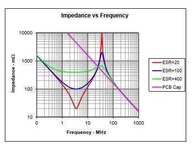
Figure 5.14 Impedance vs Frequency of Plane Capacitor and Discrete Capacitors
The plot in Figure 5.14 contains four curves. The purple curve is the impedance vs frequency of the plane capacitor by itself. The red curve is the combination of a 1 uF capacitor with an ESR of 20 milliohms and the plane capacitor. The blue curve is the combination of the 1 uF capacitor with an ESR of 100 milliohms and the plane capacitor. The green curve is the combination of the 1 uF capacitor with an ESR of 400 milliohms and the plane capacitor.
If the target impedance of the PDS was 20 milliohm this is achieved at 3.5 MHz using only a capacitor with an ESR of 20 milliohms. The problem with this solution is that at 35 MHz, there is an impedance hole that is 10 ohms! This is disastrous in a PDS. When a capacitor with more loss (100 milliohms) is used the blue curve results. The impedance at 3.5 MHz has risen to about 100 milliohms and the impedance hole has been reduced to two ohms, which is better, but still not good enough.
The green curve, using a capacitor with an ESR of 400 milliohms has finally eliminated the impedance hole. In the process, the impedance at 3.5 MHz has risen to 400 milliohms. If the target impedance was 20 milliohms this is a large miss. To get back to 20 milliohms without creating an impedance hole, it is necessary to use 20 of these lossy capacitors in parallel. This is exactly how PDS engineers determine how many of a given value of capacitor is needed.
Experience has shown that the best type of ceramic capacitors to use in a PDS are those with X5R or X7R dielectrics. This is the preferred dielectric for capacitors used in the PDS.

Minimize impedance holes
INDUCTORS OR FERRITE BEADS
Many applications’ notes instruct the designer to place ferrite beads in the power leads of devices. The usual reason given is this will “block” noise from getting onto the power pins of the device from the PDS. This has always been a patch to the real problem which is too much noise on the PDS due to the fact that it was not well engineered. There is a good chance that the advice on how to incorrectly engineer the PDS came from the same applications’ note. Earlier in this chapter, the case was made that a good PDS has a very low impedance at the frequencies of operation. A ferrite bead is a high impedance if it is going to successfully block the noise.
The origin of this rule of thumb is the late 1980s when some devices (custom CMOS devices) finally switched fast enough that they created frequencies in the EMI band. EMI technicians inserted ferrite beads in the power leads of these devices and the EMI went away. The reason is that the CMOS device did not have access to the plane capacitor of the PCB and could no longer switch fast enough to create frequencies in the EMI band.
Fast forward to the CMOS technology of today that allows us to design PCBs with SERDES (Serializer/Deserializer) that operate at rates of 28 Gb/S and higher. Suddenly, these parts need access to the plane capacitor of the PCB to do their job. Figure 5.15 is the eye diagram for the output of a 3.125 Gb/S SERDES with the eye diagram on the left taken with a ferrite bead in the Vdd lead of the driver, and on the right is with the ferrite bead removed.

Figure 5.15 Eye Diagram of a 3.125 Gb/S SERDES with Ferrite Bead on the Left and Without on The Right

Do not place Ferrite beads in the power leads of ICs
PCBS WITH NO PLANE CAPACITANCE
There are thousands of products made on four-layer PCBs with stackups like that shown in Figure 5.16. Most PC motherboards and video games are designed this way. They all have signals so fast that they need plane capacitance to do their job, yet there is none in a four-layer PCB. How is it possible for them to work properly with the absence of plane capacitance?
It might be good to point out why plane capacitors work at higher frequencies than do discrete capacitors. The reason is that the inductance of a closely-spaced plane pair is in the femtohenries while that of the best mounted discrete capacitors is rarely below 1 nanohenry.


Figure 5.16 A Typical Four-layer PCB Stackup Like That Used in a Video Game
SPLITTING GROUND PLANES
There are “rules of thumb’ that instruct a designer to split a ground plane under an A-D converter or “moat” the area around an analog circuit or switching power supply to prevent currents in the ground plane from going where they might degrade the performance of circuits nearby. None of these rules are accompanied by evidence that a real problem exists or that splitting the ground planes helps performance. It is the author’s experience that following such rules is more likely to create a problem, such as EMI, instead of solving a problem.
There are many published documents on how to treat the ground structure in a PCB. All of them maintain that the most robust way to connect grounds of components in a system for optimum performance is with a continuous, uninterrupted ground plane. It is the lowest inductance and resistance structure there is in a PCB, as long as it is not disrupted by cuts or moats.
Reference 8 below is an explanation of how to handle the “A” ground and “D” ground of an A-D converter. It is written by the chief engineer of Analog Devices and makes a clear case that creating two different grounds does not solve any problems and is likely to cause problems.

Do not cut ground planes
PDS DESIGN TOOLS
There are a number of design tools tailored for the PDS design problem. They range from Excel spreadsheet-based tools that model all of the capacitors and the planes of the PCB in two dimensions, to very complex tools that model the entire PCB and all of the loads. These tools allow the designer to simulate actual switching events, such as testing a decoupling capacitor, to see what ripple and voltage drop profiles there will be when the circuits switch on and off.
Some of the component manufacturers have even published tools that their customers can use to design their PDS. Among these is Altera who has made public such a tool that can be downloaded for free from its website. The tool is Altera PDN_Tool V10. The author has used this tool in dozens of designs with good results.
SUMMARY
With the conversion of most wide, parallel data and address buses to differential pairs and the ability to manufacture ICs with billions of transistors, the PCB design problem has gradually shifted from trying to route thousands of wires in small spaces without too much concern for signal integrity or power system design to a need to worry about how the materials affect signal quality and how the PCB stackup affects power delivery systems and EMI.
In many cases, the power delivery system design is more difficult than routing all the signals. This is due to the fact that there are often many different voltages that must fit into limited numbers of layers; they need complex sequencing and their currents are often very high with low operating voltages. Fortunately, the tools and methods are well developed to help the designer get it right the first time.
REFERENCES
- Power Bus Decoupling on Multilayer Printed Circuit Boards” IEEE Transactions on Electromagnetic Compatibility, Vol. 37, NO 2, May 1995.
- Smith, etal, “Power Distribution System Design Methodology and Capacitor Selection for Modern CMOS Technology” Published by Sun Microsystems, 1999.
- Hubing, Todd, etal, “PWB Power Structures: Theory and Design”, University of Missouri, Rolla, November 1999.
- “Power Distribution Network Design Methodologies”, Istvan Novak, IEC Publications, 2008.
- Smith, Larry, etal, “On Die Capacitance Measurements in the Frequency and Time Domains,” DesignCon 2011.
- Smith, Larry, “PDN Currents,” Published on SI Reflector. Available from Speeding Edge.
- Smith, Larry & Bogatin, Eric: “Principles of Power Integrity and PDB Design Simplified,” Prentice Hall, 2017. 8. Grounding A/D Converters‐ James Bryant, Analog Devices, EDN Page 42, March 2006


