How to Design an RF Trace Taper for Impedance Matching

Table of Contents
Take a look online for topics on impedance matching, and one of the topics you’ll inevitably run across is the use of transmission line sections for impedance matching. I wrote a piece recently that goes deep into this topic (you can read it here), and I explained why these transmission line sections can only match narrowband signals. To summarize, because the transmission line’s input impedance is very sensitive to the wavelength of a propagating signal, the matching will only be perfect at a single frequency and its higher-order multiples.
What if you have a broadband signal that you need to feed into a mismatched load? This is a major challenge in RF design, especially at very high frequencies. For example, in radar systems and in 5G systems in mmWave bands, components need to feed signals through vias to reach an antenna or a component. Depending on the relative locations between transceiver elements, RF power amplifiers, and the antenna or emitter, a via structure or a waveguide structure may be needed to route the signal.
A taper is one transmission line structure that can be used to feed a broadband signal between two transmission line structures, or between a transmission line and a load, with minimal reflection. The function of a taper is to provide the following impedance matches:
- Between two transmission lines with different widths, but same impedance
- Between two transmission lines with different widths and different impedance
- Between a transmission line and a via structure with different impedance
- Between a transmission line and some other RF structure with different impedance
- Between a transmission line and a load component with different impedance
While there is not enough room to cover every taper design situation listed above, I’ll do my best to cover two common types of tapers: linear and Klopfenstein tapers.
How RF Trace Tapers Match Impedances
An RF trace taper can be used to match two impedances, most commonly between two transmission line sections with different impedances. The goal in taper design is conceptually simple: design the trace width profile so that the reflection coefficient looking into the taper and the passband ripple are below some target value within a certain bandwidth.
Typically, you will find four types of tapers used in RF PCBs:
- Linear tapers
- Polynomial tapers
- Exponential tapers
- Klopfenstein tapers
The shapes defined in these tapers refer to the impedance profile, meaning the shape of an impedance vs. length curve when placed onto a graph. As shown below, this does not always directly translate to the same shape in the PCB. In extreme cases, even a linearly shaped taper will not have a linear impedance curve.

Two common tapers, the linear and Klopfenstein tapers, will be discussed more below.
How Tapers Work
Tapers do not pass power at all frequencies. Instead, they act like high-pass filters with a small amount of loss near DC. In fact, a taper is a limiting case of an infinite number of cascaded transmission line sections in series, each with length section approaching zero and the number of sections approaching infinity. This creates the equivalent higher-order high-pass filter behavior. In some tapers, such as the exponential taper and the Klopfenstein taper, you will see ripple in the taper’s passband.
The goal in these taper designs is to limit the reflection coefficient at the input port to be below some target value. This is done by selecting an appropriate taper length such that the taper length is much longer than the signals' wavelength. This ensures that the signal sees the smooth impedance transition along the taper, rather than a large impedance mismatch at the load end of the taper.

In some cases, there will be specific frequencies where very strong transmittance (near-zero reflection coefficient) is observed. These tend to be very high-Q passbands. An example of this effect in a Klopfenstein taper is shown below.

If you think about how these structures work, it should be clear that they are providing wavelength-dependent impedance transformations across the length of the taper. This gives us three parameters that need to be chosen when designing a taper transition between a transmission line and its destination:
- Minimum passband frequency (f-min)
- Taper width profile (dW/dl) or taper impedance profile (dZ/dl)
- Target matching impedance
Process for RF Taper Design
Above some cutoff frequency (f-min), the taper will have a very low reflection coefficient, while the reflection coefficient can be non-zero near DC. When the taper is longer, then f-min will be smaller. The actual design process is a bit more granular and proceeds as follows:
- Pick a signal frequency for your taper
- Select a trace impedance profile over the length of the taper
- Calculate the impedance gradient and the reflection coefficient gradient
- Use the results from #3 to calculate the width profile with the integral shown below
- Extend the integration limits (meaning make the taper longer) until you see acceptably low reflection at your signal frequency
Typical reflection coefficients defined from the input impedance at the taper input can be very low, less than 0.05 for certain taper profile at peak ripple within the passband. This can be seen in the example result shown above.
Types of RF Trace Tapers
Linear Taper
The term “linear taper” refers to two types of tapers: a taper with a linear shape, and a taper with a linear impedance gradient. For microstrips that are sufficiently wide as defined in the classic effective Dk equation, the shape of a taper with linear gradient will also be very close to linear.
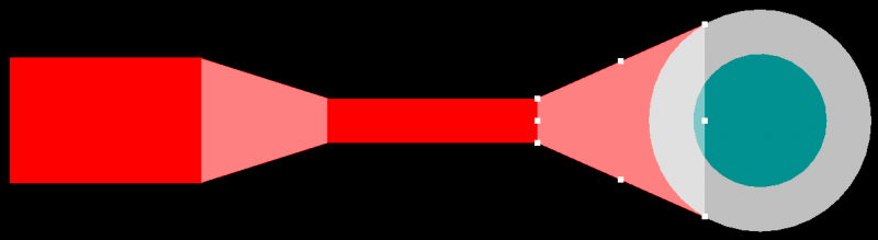
An example with a linear taper shape is shown below. These taper shapes were applied as polygons between different elements in the PCB. The length is chosen based on the required f-min value for the passband as described below.
To start a linear taper design, first recognize that a taper has a characteristic impedance that is a function of the length along the taper. Using the source-side and load-side impedances, we can define the following function for a linear impedance profile along the taper, where L is the total length:

Now we have everything needed to calculate the reflection coefficient along the length of the taper. To do this, we apply a phase shift along the length of the taper as a function of the propagation constant and the impedance profile defined above. This requires evaluating the following integral:

The above integral assumes that your taper will be designed short enough that the losses can be ignored.
This integral is used to calculate the reflection coefficient for any impedance profile. Here we have an angular frequency and the speed of light along the transmission line in the exponential function. The resulting expression evaluated from this integral gives you a reflection coefficient for different pairs of L and ⍵. You can essentially pick your signal’s frequency and then evaluate the above integral numerically by extending the integration limits until you get an acceptable value for the reflection coefficient. To help you run through the above integral, you can download a microstrip trace taper calculator worksheet for use in Excel.
Once you have the reflection coefficient, you can use it to calculate the S-parameters by comparing with your feedline impedance. An example is shown below.
Linear Taper Example at 80 GHz
The simulation result from Simbeor outlined below shows S11 data for a linear taper targeting a 80 GHz application. This taper is reaching the upper limits of what would typically be fabricable with thin laminates in an RF board with a digital interface, but the result shows that it is possible to design tapers with very high frequency of operation and moderately high bandwidth. As of the time of writing this article, the board that includes this taper design is in fabrication.

In this example linear taper design, we have very desirable impedance matching from 77.5 GHz to 83.75 GHz, or nearly 10% of a 80 GHz carrier, where the bandwidth limit has been set to S11 = -10 dB. This is far superior bandwidth compared to what you would see with a practical quarter-wavelength transmission line for impedance matching.
The parameters for this taper are:
- Taper type: microstrip
- Taper length: 15.3 mm
- F-min: 67 GHz
- Maximum reflection in passband: 0.01
- Target matching impedance: 37.5 Ohms @ 80 GHz
- Feedline impedance: 50 Ohms
Why do we not get wider bandwidth in the above result? The reason is that the load impedance in this example does not have a flat impedance spectrum, it does vary strongly around 80 GHz, so the condition for matching at a different frequency is not met with this taper. In this example, the load is a through-hole via structure that must transfer an 80 GHz signal across a 62 mil board with 8 layers. The via impedance varies with frequency around the 80 GHz carrier frequency, so we won’t have perfect matching very far from 80 GHz. This is exactly what we see in the above simulation result.
Klopfenstein Taper
This type of trace taper takes a different approach to determining the design parameters. Instead of setting a specific taper impedance or length profile and trying to minimize the input impedance, the mathematical procedure sets an upper limit on the allowed S11 value and returns the required profile needed to match input and output impedances. The length is set by the wavelength being targeted for impedance matching. These profiles can typically return impedance matching that is well below -20 dB throughout the passband.
Klopfenstein tapers have a nonlinear profile as shown above. The mathematics behind this is not very complex, but it is extensive with a lot of values to track along the way. Take a look at this page from Microwaves 101, it contains a spreadsheet that will calculate passbands and ripple for Klopfenstein tapers.
Other Taper Profiles
Technically, any impedance profile or shape profile could be used to design a taper. If you follow the procedure outlined above for the linear taper, and you use the reflection coefficient equation outlined above, then you can calculate the reflection coefficient for any taper impedance profile.
If you want to start with a specific width profile, you can get the impedance gradient using the chain rule:

This is because the characteristic impedance is a function of the width, and the width is also a function of the length. In this case, you can pick either a dW/dl taper width profile, or a dZ/dl impedance profile. As an example, an exponential impedance profile will have a sinc function passband with specific input frequencies that will produce nearly zero reflection coefficient.
The dZ/dW derivative should be known; it can be easily calculated directly from classic equations for microstrip and stripline impedance (assuming TEM propagation). For more complex transmission lines, the derivative will also be more complex and may require taking the derivative of a elliptical integral of the first kind (e.g., see Wadell’s textbook Transmission Line Design Handbook for examples involving coplanar lines).
Once you’ve determined your taper width profile, you can easily place it in your PCB layout ith the CAD tools in Altium Designer®. You can draw the taper directly in a PCB layout, or you can import it from another drafting program and place it as a copper region. When you’ve finished your design, and you want to release files to your manufacturer, the Altium 365™ platform makes it easy to collaborate and share your projects.
We have only scratched the surface of what’s possible with Altium Designer on Altium 365. Start your free trial of Altium Designer + Altium 365 today.

About Author
Related Resources


Related Technical Documentation


Take advantage of the world's
most trusted PCB design system.
One interface. One data
model. Endless possibilities.
Effortlessly collaborate with
mechanical designers.
The world's most trusted
PCB design platform
Best in class interactive
routing
View License Options
Thank you, you are now subscribed to updates.