DIY PCB Stencil Made Easy with Proper Board Layout Software

Table of Contents
- Utilizing a Paste Stencil Design for Faster PCB Assembly Starts Within Altium Designer
- Altium Designer Takes the Precise Approach to DIY PCB Stencils
- Moving a Design from Layout to Production with Ease
- Altium Designer Uses Advanced Layer Stack Technologies
- Use Design Software that Works With Your Design Needs
Fabrication, assembly, and manufacturing can all become a breeze so long as you’re using the proper PCB design software. Make sure that anything you use in those processes, like what is a stencil for PCB, is accounted for with your CAD tools. In this article, we are going to explore what is stencil in PCB and the types of stencil for PCB.
ALTIUM DESIGNER
PCB design software is responsible for enabling your designs to be produced with ease.
The purpose of PCB stencils software is to quickly install solder paste onto circuit boards, and there are a lot of names and approaches to this concept: laser-cut stencils (aka laser stencils), stainless steel metal stencils, full-sized and mini stencils, stencil frame, and paste stencil, just to name a few. But how to use a PCB stencil and to make use of a stencil printer doesn’t need to be as confusing as it sounds.
Moving your PCB design from prototype to production requires developing a solder mask layer and the paste mask layer or stencil. The solder mask layer designates areas of the PCB for covering with solder resist ink. Paste mask layers—or stencils--mark the locations for applying solder paste to the PCB. Developing solder paste stenciling requires specific methods to ensure that the PCB design moves correctly from prototype to production.
When working with your circuit board to make your board work with its manufacturing and solder paste requirements, considering stencil program thickness, stencil PCB design, and the reflow oven are pieces that might not come to the forefront of a designer’s mind. But a printed circuit board should have its design checked for both ease of layout and ease of production, that’s where a strong CAD tool can come from.
Utilizing a Paste Stencil Design for Faster PCB Assembly Starts Within Altium Designer
When you and your design team work with frameless stencils, prototype SMT stencils, or rework stencils, you need a PCB stencil maker and design software that provides uniformity, efficiency, and reliability. Altium Designer offers a unified approach for layer stacks, stencil materials, marker identification locations, and foil thickness. In addition, Altium Designer ensures the correctness of your surface mount device connections by assisting with your project through the entire design process.
The tools found within Altium Designer assist with avoiding problems with the circuit board stencil, whether it’s a laser-cut stainless steel metal stencil, a simple mini stencil, or any DIY PCB stencil in between. As you work with Surface Mount Devices, the size of the components decreases the effectiveness of solder paste stencil printers. Incorrect stencils can lead to problems with PCB reliability. Poor stencil resolution or stencils with ragged edges decrease the joint edge definition and can lead to the over-application of solder paste. The uneven distribution of solder paste can allow bridges to form and cause shorting.
Altium Designer Takes the Precise Approach to DIY PCB Stencils
Selecting the proper foil thickness depends on the types of devices loaded onto the PCB. For example, some component packages—such as 0.020” pitch Small Outline Integrated Circuits (SOIC) need a thinner solder paste stencil than 0.050” pitch SOICs. With solder paste stencil program thicknesses ranging from 0.001” to 0.030” and foil thicknesses ranging from 0.004” to 0.007”, controlling the volume of solder paste deposited on the board and preventing poor solder joints can become a design issue. Altium Designer automatically calculates the precise stencil and foil thicknesses along with the precise stencil aperture dimensions and marker identification locations for your Printed Circuit Board design and components.
- Using a circuit board stencil in your PCB manufacturing will require some planning and foresight. Learn more about solder paste stencil PCB guidelines.
- Adapting your board to the shape and size you need for your solder pour and product requires intuitive design software. Learn more about changing board sizes in Altium Designer.
- Don’t let your board fall victim to solder bridge shorts. Learn more about solder bridge shorts.

Working through your board shapes can ensure that you understand what soldering needs your circuit board has. Alt text: Printed circuit maintaining)
Moving a Design from Layout to Production with Ease
The Layer Stack Manager dialog in Altium Designer gives you the precision tools for configuring the layers of the board. You can access the Layer Stack Manager from the toolbar and choose either the Simple or Advanced Layer Stack Manager dialogs. When using the Simple dialog, you gain the features and functionality for managing the layers in the stack for a simple, rigid PCB. The Advanced Mode dialog offers the additional controls used for adding and managing multiple sub-stacks for rigid-flex PCBs. With both dialog options, Altium Designer provides the Custom, Layer Pairs, Internal Layer Pairs, and Build-up options for building the board.
Altium Designer Uses Advanced Layer Stack Technologies
The Layer Stackup Setting allows you to select the dielectric layer and the location of the stack while you can use the Drill-Pair Manager to configure the required drill pairs for the active layer stack. Settings for the Dielectric Manager allow you to display the type of layer and use the None, Core, Prepreg, Surface Material, and Film options to specify the Solder Mask type.
As you work with the Solder Mask Layer settings, you can name the solder mask layers, specify the mask layer material, set the thickness of the solder mask, and specify the dielectric constant for the solder mask material. You can use the Layer Stack Preview to gain a graphical preview of the stackup.
- Layer stack management is a difficult feature to master in board design software. Learn more about optimizing your layer stack.
- With printed circuits incorporating high-speed designs more frequently, you’ll want to make sure your layer stack knowledge can accommodate. Learn more about organizing a layer stack for high-speed designs.
- Rigid-flex designs add a layer of complexity to your layer stack management. Learn more layer stack management for rigid-flex designs.
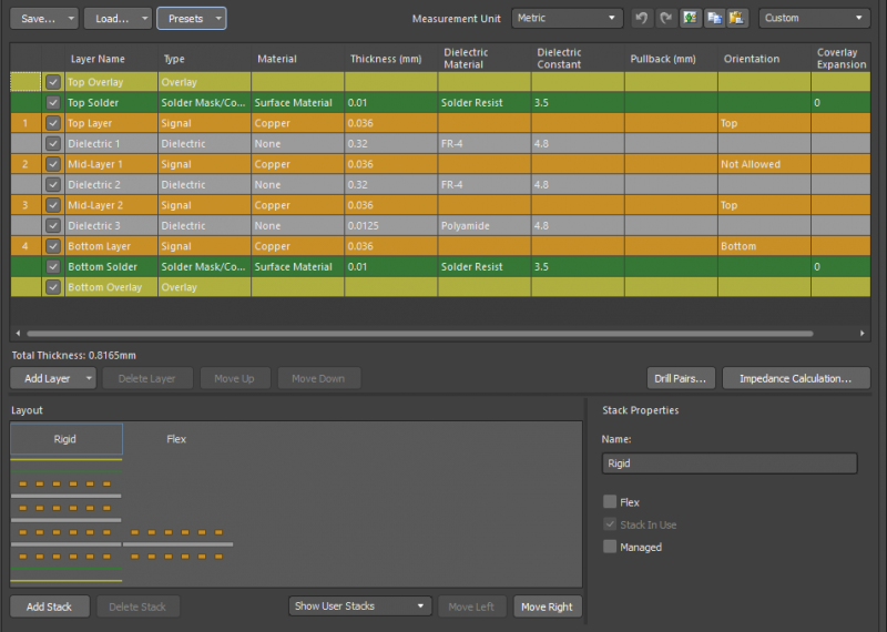
Organizing your layer stack will help to ensure that your design succeeds without a hitch. Alt text: Screenshot capture of Altium Designer Layer Stack for printed circuit management)
Use Design Software that Works With Your Design Needs
Laser-cut stainless steel foils create openings for every surface mount device found in the PCB design. Before you can arrive at placing the openings, creating solder mask-defined (SMD) windows for the thermal pads, and carefully aligning the circuit board stencil with the PCB, you need tools that ease the process of building prototype cards. Altium Designer’s PCB Library Editor provides the tools needed to reduce stand-off variability, improve reliability, and ensure proper via counts.
Standard Pad Objects within Altium Designer can provide round, rectangular, rounded rectangular, and octagonal pad shapes. You can size the pad shapes in the X and Y directions and use round or slotted holes. Because new component footprints may require custom pad shapes, Altium Designer also allows you to place other design objects such as fills, arcs, lines, or regions to build the copper shape used for the custom pad.
You can use the Solid Region object as a polygonal object to develop custom pad shapes. In addition, you can use the Guide Manager to define four Point Guides at required locations. Altium Designer also provides another option for creating custom pad shapes. By using lines and arcs, you can define a closed outline of the shape and then convert the outline to a Solid Region. After selecting the Lines and Arcs, you can run the Create Region from Selected Primitives command from the Tools and Convert pull-down menus.
Altium Designer Allows You to Work with Custom Pad Shapes
Altium Designer allows you to calculate Solder and/or Paste Masks for any primitive object. With the tools found in Designer, you gain the option of calculating the Solder and/or Paste Mask with a user-defined amount or using the rule system. The Properties panel allows you to enable the correct Mask Expansion control settings.
Some mask openings cannot use a calculated mask. Working with a manually defined mask begins with placing suitable design objects on the required Mask Layer. Defining the mask occurs in the negative with placed objects defining openings in the Solder Mask layer.
You can define the solder mask by using track and arc primitives with the Altium Designer PCB Library Editor. After setting the active layer to solder mask, the Editor allows you to draw arcs around vias, create lines along the exterior of the thermal pads and draw additional intersecting tracks for the solder mask pane line. From there, you can select the primitives and use the Tools menu to create a region from the selected primitives.
Altium’s toolset allows you to create solder mask expansions for each via hole and to copy the SMD windows from the solder mask layer to the solder paste layer. The Altium software also detects and resolves routing connections to any copper object. In addition, you can use polygon thermal connection spokes during the design of a custom pad. Small pads within the software work as polygon connection points. Then, you can use Altium Designer to associate each new footprint with a device and render a 3D image of the PCB.
- Interactive routing is just one of the many tools at your disposal to help solder and soldering become an easy process. Learn more about Altium Designer’s Interactive Routing.
- Smart component placement will enable your design to flourish without the added hassle of having to find the right component to match it. Learn more about Altium Designer’s Smart Component Placement.
- Don’t forget that any design you create ought to have plans to be produced, and with those plans comes the necessity for output modes like the Gerber file and BOM. Learn more about Altium Designer’s Real-Time BOM Management.
Altium Designer automatically calculates everything that you need for producing DIY PCB stencils. The powerful software establishes a unified approach to PCB design and development with tools that include Schematic Editor, ActiveBOM, Interactive Routing, and Native 3D PCB Design. Altium Designer includes extensive component libraries that connect you to vendors in real-time and is the best PCB stencil maker on the market.

About Author
Related Resources


Related Technical Documentation


Take advantage of the world's
most trusted PCB design system.
One interface. One data
model. Endless possibilities.
Effortlessly collaborate with
mechanical designers.
The world's most trusted
PCB design platform
Best in class interactive
routing
View License Options
Thank you, you are now subscribed to updates.