Use PCB Routing Tools With an Integrated Trace Length Matching Calculator

Table of Contents
If you’re a mechanical or electrical designer, you need CAD tools that provide accurate trace length and geometry calculations. Once you start working with high-speed or high-frequency circuits, propagation delay and skew become critical points to consider as you need to make sure your signals are properly timed throughout your nets. Altium Designer is the only PCB design package that includes an ultra-accurate trace length calculator for PCB trace length matching vs. frequency. This feature interfaces directly with your other design tools using a rules-driven design engine.
ALTIUM DESIGNER
The only unified PCB design package with an integrated trace length calculator and PCB trace length matching vs. frequency capabilities.
When designing high-speed boards, you need to worry about two things: length matching in parallel nets and differential pairs, and specified trace lengths to comply with specific routing standards. Trace lengths for high-speed signals are often determined prior to layout. Maximum lengths can be determined manually by analyzing a signal’s rise or fall times with respect to propagation delay, or they can be inferred from an allowed impedance mismatch; the two approaches are equivalent.
If this all sounds complex, there are solutions that can help. Determining trace impedance and propagation delay in PCB traces takes a trace length calculator and impedance profiler tool, and these features work best when they are integrated into your PCB design software. With Altium Designer, you can easily determine trace impedance, propagation delay, rise times, and PCB trace length matching vs. frequency in your new circuit board. You’ll have everything you need to route and analyze your design in a single program.
Why Do I Need to Know My Trace Lengths?
Different boards have different requirements on trace lengths and on the sizes of conductive elements in general. For example, if you’re designing a printed antenna on your board, you’ll need to carefully verify the size of your antenna to ensure it will resonate at the desired frequency. If you’re working with data in a set of parallel nets, you’ll need to make sure traces are length-matched within allowed tolerances.
Any electronic signal requires a specific amount of time to travel through a conductor from its source to its destination. An electronic signal, whether digital or analog, travels along a trace with a velocity that equals the speed of light in the PCB substrate material. This speed, in turn, depends on the effective Dk value of the trace. The Dk value for the PCB substrate, the geometry of the trace, and the geometry of the conductor all determine the speed of signals in your traces.
Keeping Lengths Within Limits with a Trace Length Calculator
Many high-speed routing standards require a trace length to remain under some maximum. When routing a board, you need to see your trace lengths as you layout your board. Not all circuit boards are built on FR4, and a complex layout creates multiple parasitics that need to be included in propagation delay calculations. To make sure you’re routing within high-speed routing standards, your PCB design software needs to calculate the characteristic impedance and propagation delay of your traces using the substrate Dk value and any parasitics in your layout.

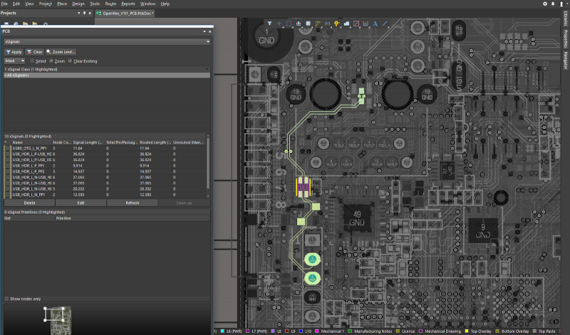
You can identify traces and calculate the maximum trace lengths with Altium Designer.
Forget About 3rd a Party PCB Trace Length Calculator
In reality, there is no single formula for calculating the exact trace length you need in your printed circuit board. When your PCB design software includes an automated trace length calculator, you can immediately view lengths for individual traces or for all traces in a net. You’ll be able to check your trace lengths against the propagation delay tolerances in your traces. The days of using an external tool or command-line based CAD tools to measure trace lengths are over.
- When your board gets packed with corners, you’ll need to route around bends and corners in your board. Learn about routing with bends and corners in your PCB design software.
- Multilayer boards can offer some convenience during the routing. In some cases, it may be better to opt for a longer trace instead of routing through a via. Learn more about choosing between longer traces and routing through vias.
- Some high-speed signaling standards require individual signals to remain within length limits to prevent excess loss. Learn more about incorporating length matching into your design rules.
A Trace Length Calculator for Differential Pairs and Nets
Propagation delay mismatches in different nets are notorious for producing signal synchronization problems. When two ends of a differential pair or a group of signal nets are mismatched, there will be excess skew between signals. This causes the signals to become desynchronized at the receiver.
In differential pairs, this prevents common-mode noise cancellation at the receiver and alters the desired signal level. In parallel nets, this causes signals to reach the receiver at different times, which causes gates to latch in the incorrect order. When you can quickly match lengths with a PCB trace length calculator, you can prevent these signal problems and ensure your signals are received properly.
Trace Length Tolerance Matching in High-Speed PCB Design
Impedance-controlled routing and trace length matching really go hand-in-hand. The easiest way to ensure traces within a signal net remain matched, is to increase the length of all traces in a net so that they match the length of the longest trace. Trace length matching in your PCB is much easier when you use the right design software. Built-in trace length matching should allow you to easily meander traces in a serpentine or accordion pattern as they travel from source to load.
There is always a danger that a trace makes a transition to transmission line behavior, but you can prevent reflection from loads due to impedance mismatch when you use impedance-controlled design techniques. This requires explicitly defining the trace geometry with respect to the dielectric constant of the substrate material. This helps ensure that your microstrip trace impedance and stripline trace impedance will match to the desired value within a predefined tolerance interval.
- When you need to length-match meandered traces, a built-in PCB trace length matching calculator makes impedance-controlled routing easy while ensuring differential pairs and parallel nets are matched within timing tolerances. Learn more about trace length matching with meandering styles.
- Working with an impedance-controlled board requires building the proper layer stack for your PCB. Learn more about building your layer stack for impedance-controlled design.
- Working with high-speed and high impedance boards requires implementing high-speed design techniques and simulations into your PCB design workflow. Learn more about incorporating signal analysis into your PCB design workflow.

You can configure nets in a fly-by topology with and ensure PCB trace length matching in Altium Designer.
PCB Trace Length Matching vs. Frequency with Altium Designer
Matching trace lengths at specific frequencies require understanding dispersion in your PCB substrate material. Because trace, source, and load impedance mismatches are a critical concern in high frequency design, you need a PCB trace length matching vs. frequency calculator that determines propagation delay and impedance at any frequency. Your calculator should determine impedance directly from your stackup. Signal analysis and simulation tools will give you an immediate view of any signal integrity problems at any frequency. You can iteratively determine the best components to use in a variety of termination schemes.
Define Signals Tolerances Using Rules-Driven Design
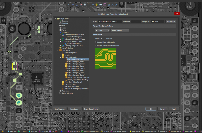
Altium Designer’s rules-driven design engine allows you to define trace length tolerances in differential pairs and across signal nets. As you route your board, the built-in trace length calculator will check your routing against your design rules and flag errors for correction. The trace length calculator in Altium Designer provides PCB trace length matching vs. frequency, which helps prevent skew in wideband signals.
- The rules-driven design environment in Altium Designer integrates all your design features with a trace length calculator and impedance calculator. These features also allow PCB trace length matching vs. frequency with a single set of routing tools.
Learn more about the rules-driven design engine in Altium Designer.
- Differential pairs require defining accurate net clearances and trace lengths to ensure maximum crosstalk suppression. Learn more about differential pair routing in Altium Designer.
- The interactive routing features make length matching easy by allowing you to apply phase and delay tuning to your high-speed signal nets. Learn more about enhanced length matching with phase and delay tuning.
Working in an integrated design environment might seem challenging, but Altium will be there with plenty of resources to help you succeed. Between an extensive knowledge base, the AltiumLive forum, podcasts with PCB design industry experts, and detailed feature tutorials, you’ll have access to the resources you need to enter the world of modern PCB design.
Altium Designer also includes a data management suite, production planning features, and a set of world-class schematic design features. Whether you’re a professional PCB designer or you’re just getting started in the wide world of PCB design, Altium Designer has something for everyone.
Altium Designer is more than just a design tool. Altium Designer on Altium 365 delivers an unprecedented amount of integration to the electronics industry until now relegated to the world of software development, allowing designers to work from home and reach unprecedented levels of efficiency.
We have only scratched the surface of what is possible to do with Altium Designer on Altium 365. You can check the product page for a more in-depth feature description or one of the On-Demand Webinars.


