IPC Classes and Complying with IPC Standards for PCB Design

Table of Contents
Whether you work in electronics design, manufacturing, or even defense, the alphabet soup of standards organizations is extensive and may seem daunting. The IPC standards are among the most widely accepted and important standards for PCB design and manufacturing. IPC standards will influence how a designer creates their board and how they will prepare it for production in different industries. These standards are meant to ensure performance and reliability and are accepted by a number of industries.
Although the IPC standards are vital for ensuring design performance, reliability, and quality, they are not the only standards that matter for all industries. Other important standards organizations that influence PCB design include ASME, ANSI, IEC, MIL-PRF, and other specialty standards for specific products. No matter which standards matter for your design, the best PCB design software can help you comply with your standards by encoding design requirements as design rules.
ALTIUM DESIGNER®
The only unified PCB design suite with design and verification features that can be tailored to IPC standards.
Among the many electronics standards organizations, the organization that all designers should be aware of is IPC. These industry standards are designed to ensure the reliability and manufacturability of printed circuits and other electronic assemblies. The goal of the IPC standards is to ensure that electronics products are reliable, safe, and manufacturable. No matter which industry vertical or market segment you work in, IPC likely defines standards that specify important requirements for your products.
Very few people have ever read the entirety of the IPC standards, simply due to their breadth and depth. If you are a PCB designer, there are some very important standards with which you should become familiar. When you use the right design software with integrated compliance tools, it may be easier than you think to comply with IPC standards and design to different IPC product classes. Altium Designer’s integrated design rule engine lets you define important IPC standards as design constraints, which helps you comply with these important standards.
IPC Standards on PCB Design and Manufacturing
The IPC standards include multiple manufacturing requirements for all aspects of a printed circuit board. These manufacturing requirements ultimately translate back to design requirements, and designers need PCB design software to help ensure their boards will be compliant with IPC design requirements. Some examples include via and microvia manufacturing, solder joint strength requirements, solder mask material and thickness, material properties for substrates, and several other manufacturing requirements.
What IPC Sections are Relevant to PCB Design and Manufacturing?
There are many sections of the IPC standards, and not all sections are applicable to every circuit board design. In addition, each standard is a very long document that includes a range of requirements for designers, manufacturers, or both. Some of the important IPC design standards include:
- IPC 2221: Establishes some generic design and performance requirements in PCBs and other forms of component mounting or interconnecting structures.
- IPC 4101: Defines material requirements for PCB laminate materials and other materials used to build stackups.
- IPC 2152: A newer standard that defines current carrying requirements in copper traces and planes in a number of different applications.
- IPC 4761: Covers design guidelines for via protection to ensure reliability, manufacturability, and quality.
- IPC 6012: Defines generic performance requirements as compiled from IPC 2221, IPC 4101, and other quality requirements. The related IPC 6013 standard applies the same ideas to flex circuit boards.
- IPC-A-600 series: Defines acceptance metrics for printed circuit boards, as well as the three standard IPC Classes for various printed circuit board assemblies.
- IPC 7351: Specifies footprint and land pattern requirements for SMT components. Component manufacturers use these specifications when designing their land patterns to ensure solderability and reliable electrical connections.
- IPC-1752A: Material Declaration Management standard defines reporting formats for data exchanged between designers, distributors, and manufacturers.
There are many other standards that affect design, manufacture, and qualification of printed circuit boards, but not all of these are critical for PCB designers. The important design requirements from the list above will largely affect things like clearances, testing requirements, feature sizing, mechanical design requirements, and protection requirements to ensure high quality.
The important point to understand in your design software is to encode these requirements into your design rules so you can quickly evaluate your physical layout before you prepare for fabrication and assembly. The best PCB design tools will take these requirements directly from your design rules and instantly evaluate your board in any application.
- In some designs, such as HDI circuit boards, you’ll need to use vias with tented vias or VIPPO in your landing patterns.
Learn more about designing via protection under the IPC-4761 standard.
- The IPC-2152 standard defines the recommended relationship between trace width and current capacity for different copper weights in your traces.
Learn more about IPC 2152 and designing the appropriate trace width.
- IPC-7351 defines standards on land patterns for component footprints, and component designers should pay attention to these standards to ensure manufacturability on circuit boards.
See how you can create IPC-compliant footprint models in Altium Designer.

You can design an IPC-7351 compliant component footprint in Altium Designer.
What Do PCB Designers Need to Know About IPC Classes?
The IPC standards define four product classifications. Class 1 defines requirements for general printed circuit boards with a limited life and simple functions. These boards are meant for one-time use or throwaway products. Class 2 defines design requirements for electronic products that require extended service life and on-demand performance. These boards tend to have more complicated functions than would be found in simple devices and are often part of a larger system, such as a computer or television.
Class 3 PCBs have tighter in-manufacturing tolerances and more stringent reliability requirements as opposed to Class 1 and Class 2 boards. Someone that is not a professional designer is likely designing a Class 1 circuit board. More complex products tend to be built to Class 2 or Class 3. IPC Class 3/A takes the Class 3 reliability requirements and applies them to military and/or aerospace electronic products. Other important standards organizations for military products include ISO, MIL, FAA, and SAE.
To get a more thorough view of IPC standard requirements as they apply to PCB manufacturing, you can view the IPC’s manufacturer’s checklist.
Differences Between IPC Class 2 and Class 3
Products defined as Class 3 must be built according to criteria that includes plating thickness, laminate/solder mask selection, PCB manufacturing processes, material qualifications, and quality inspection. The major differences between Class 2 and Class 3 are in the component placement requirements for SMT components. Class 3 places stricter cleanliness requirements on the assemblies, defines a definite plating thickness in through-hole vias, and plating thickness on the surface of PCBs.

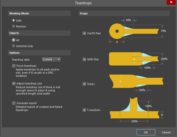
Teardrops are used in IPC Class 3 PCBs as a method to prevent breakout where traces meet vias.
PCB designers need to address all these fabrication requirements during the design phase. Addressing these issues as you design will prevent a redesign once you send your board to your manufacturer. Following important IPC standards on design and fabrication also helps ensure you have the highest possible board yield.
- Every product contains defects, but these defects should be minor enough that your board will not have major problems during fabrication.
Learn more about appropriate tolerances in different IPC class products.
- The IPC-6012E standards on annular rings for Class 3 products are designed to ensure your vias have the appropriate mechanical strength to withstand thermal expansion during operation.
Learn about designing annular rings on vias to comply with IPC 6012E for Class 3 products.
- Design data for an IPC product class will need to be exported into standard manufacturing file formats. The IPC-2581 is one popular vendor-neutral file format.
Learn more about PCB production file formats, including the IPC-2581 file format.

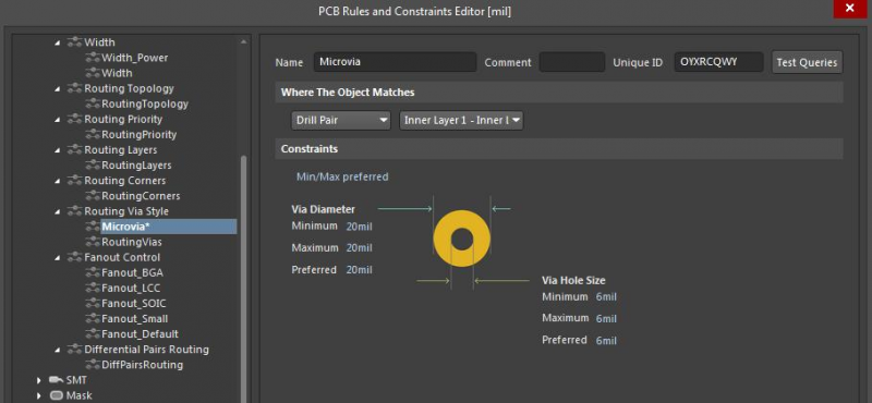
Via design is an important aspect of reliability in different IPC class products.
Other Important Industry Standards for Electronics
Much like other industries, major electronics companies have collaborated to define a range of standards governing electronics design, fabrication, assembly, and testing. Some of these industry standards are more stringent and go far beyond the IPC standards for PCB design. Some of these other groups of standards include:
- International Standards Organization (ISO): This set of standards largely covers manufacturing and quality control, but it also extends requirements to specific products and industries (e.g., ISO 13485 for medical devices.
- International Electrotechnical Commission (IEC): A safety and performance standards organization that stresses international cooperation on electrical and electronics standards.
- Underwriter’s Laboratory (UL): A standards organization that qualifies electronic products for electrical safety.
- American Society of Mechanical Engineers: A general set of design and reliability standards that can apply to any electronics assembly, particularly in electromechanical systems.
- Military Performance Specification (MIL-PRF): These standards apply mechanical performance requirements and reliability standards to electronics for military equipment and defense systems.
- Military Standard (MIL-STD): A broad set of standards that defines a range of requirements on military hardware. This includes testing requirements for military electronics.
The design standards specified directly and indirectly by these organizations can be encoded as design rules in Altium Designer, just like your other important IPC standards for PCB design. It is up to you as a designer to determine which standards are most important for your product. Altium Designer includes all the design tools you need to ensure your physical layout will comply with any of these design requirements thanks to its integrated underlying design engine.
Altium Designer Helps You Comply With Any PCB Design Standards
As you create your circuit board, the online DRC engine in Altium Designer checks your PCB layout against your design rules as you create your circuit board. Every design feature in the program reads from these design rules as you build your board. The verification features automatically check your design against standard and customized design rules, helping you remain compliant with IPC standards for PCB design.
- Altium Designer’s complete set of design tools are built on a rules-driven design engine. This allows you to define IPC standards for PCB design and different IPC classes as design rules and constraints. Your layout will be automatically checked against your design rules as you create your board.
Learn more about the rules-driven PCB design environment in Altium Designer.
- As a professional designer, you might want to increase your PCB design expertise. Taking an IPC CID certification can help you improve your circuit board design skills.
See how you can benefit from an IPC CID certification as a designer or manufacturer.
- Altium 365 gives design teams a way to collaborate in a securely managed cloud environment. You can instantly share your design and production data through Altium Designer or on the web.

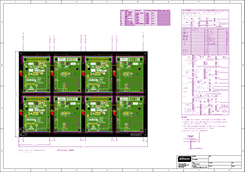
You can ensure this panel obeys important IPC standards for PCB design when you use Altium Designer.
With the rules-driven design engine in Altium Designer, you can ensure important IPC standards for PCB design are automatically checked as you create your circuit board. No matter which IPC class you want to design to, you’ll be able to create high-quality circuit boards and take them to production with Altium Designer.
Altium Designer on Altium 365 delivers an unprecedented amount of integration to the electronics industry until now relegated to the world of software development, allowing designers to work from home and reach unprecedented levels of efficiency.
We have only scratched the surface of what is possible to do with Altium Designer on Altium 365. You can check the product page for a more in-depth feature description or one of the On-Demand Webinars.


