
在 PCB 上处理房间
摘要
 Room(房间)是在 PCB 某个表面层上定义的一块区域。Room 用于定义该板区内的设计要求,例如:these components must be in this area,或 route these nets this width,或 use routing vias of this size。
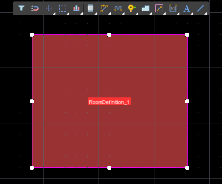
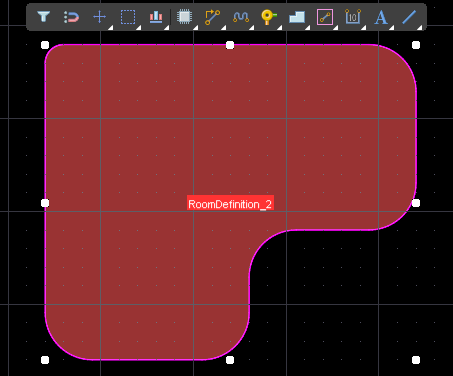
Room 的放置方式与其他多边形对象类似,可以是矩形,也可以是多边形形状。
Room 除了作为板上一个带名称的 X-Y 形状存在外,还会自动生成一条带名称的 Room Definition 设计约束(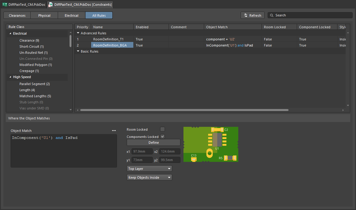 )。Room Definition 约束中的设置用于定义:该 Room 适用的 objects,这些对象是否需要保持在 Room 的 inside or outside,以及该 Room 应用到的 layer。
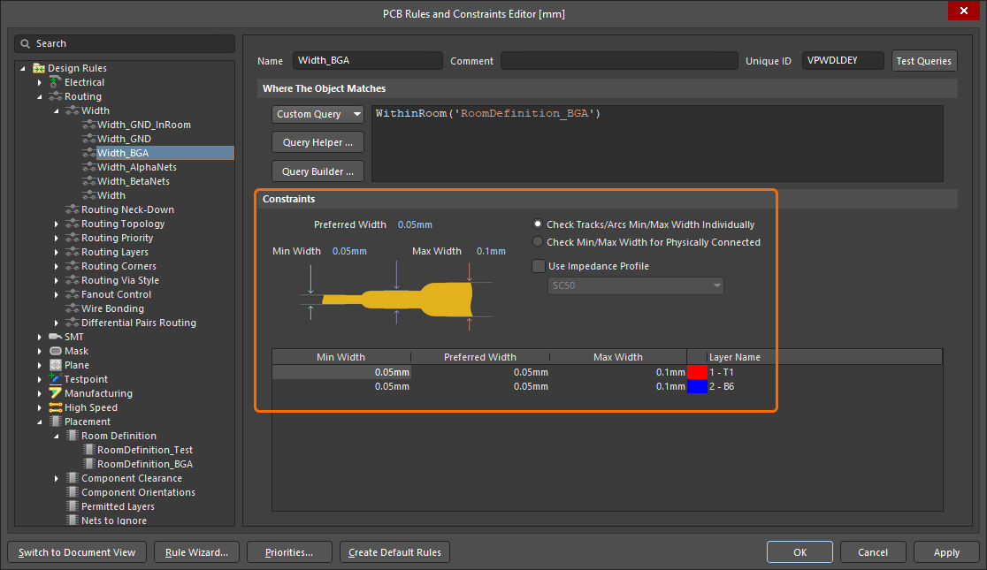
除了 Room Definition 约束直接指定的简单 keep these objects in (or out) 要求之外,Room 还可用于定义板上一个应用其他设计约束的区域。例如,BGA 下方的布线可能需要特定线宽(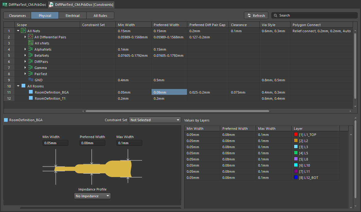 );或者,BGA 下方的差分对布线可能需要应用特定的阻抗配置文件(
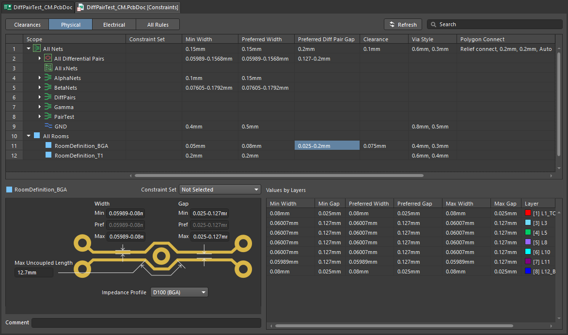 )。
)。
可用性
Room 只能在 PCB Editor 中放置/创建。可使用以下方法创建 Room:
-
从 Design » Rooms 子菜单中选择所需命令,然后交互式定义 Room 形状(如果选择的是 Place 命令),或自动创建 Room(如果选择的是 Create 命令)。
-
添加一条新的 Room Definition 设计约束,然后编辑新的 Room 约束,再点击 Define 按钮以交互式定义多边形 Room 的形状。
-
使用 Tools » Convert » Create Room from Selected Primitives 命令,基于由一组走线/圆弧形成的(已选中)闭合轮廓来创建 Room。
-
在原理图到 PCB 设计同步期间自动创建 Room。了解更多关于 自动生成的 Room (包括如何禁用它们)。
创建 Room
在 PCB 文档中创建 Room 的流程取决于你是交互式放置/创建 Room,还是使用了哪一种具体的放置/创建方法。
 放置或创建 Room 有多种技术可用。
Interactive Room Placement
矩形或多边形 Room 可放置在设计的顶层或底层。注意:即使在任意活动层时都可以放置,但其适用层是在 Room Definition 设计约束中指定的。
矩形 Room
启动 Design » Rooms » Place Rectangular Room 命令后,光标会变为十字准星,并进入 Room 放置模式。放置过程按以下步骤进行:
-
单击或按 Enter 以锚定 Room 的第一个角点。
-
若要在放置过程中即时编辑关联的 Room Definition 约束 属性,请在放置时按 Tab 键。
-
移动光标调整 Room 大小,然后单击或按 Enter 键以锚定对角的另一角点并完成 Room 放置。
-
继续放置更多 Room,或右键单击/按 Esc 退出放置模式。
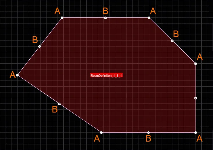
多边形 Room
启动 Design » Rooms » Place Polygonal Room 命令后,光标会变为十字准星并进入 Room 放置模式。放置过程按以下步骤进行:
-
定位光标并单击,以锚定 Room 的起始点。
-
定位光标并单击,以锚定一系列顶点,从而定义 Room 的多边形形状。
-
放置最后一个顶点后,右键单击或按 Esc 完成 Room 放置。无需手动闭合多边形,因为软件会自动将起点与最后一个点连接以完成形状。
-
继续放置更多多边形 Room,或右键单击/按 Esc 退出放置模式。
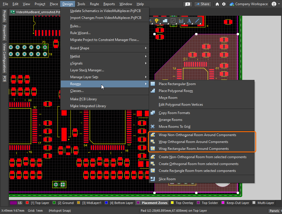
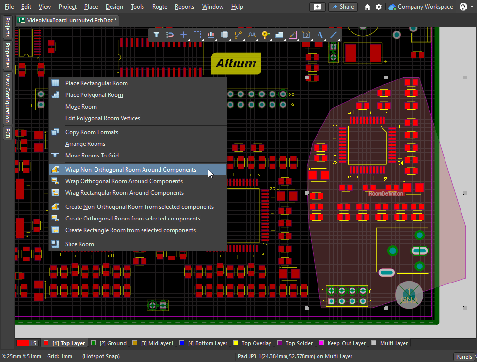
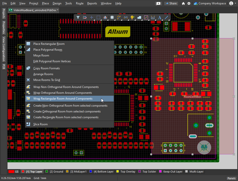
Based on Selected Components
如果元件已经在板上摆放好,并且你希望创建一个适配其摆放的新 Room,请使用三个 Create xxx Room from selected components 命令之一。基于当前在设计空间中选中的元件,这些命令可自动创建非正交、正交以及矩形 Room。每种情况下的创建方法相同:
-
选择你希望为其创建 Room 的所有元件。若要从原理图中选择 PCB 元件,请运行 Tools » Cross Select Mode 命令,然后在原理图上选择这些元件。
-
在 PCB 编辑器中,启动相应的创建命令(Design » Rooms » Create xxx Room from selected components)。 系统会自动创建一个包含所选元件的元件类(除非已存在)。
-
随后会创建所选类型的 Room,并将该 Room 的 Room Definition 设计规则自动关联到所创建的元件类。
-
Room 会根据元件的选择矩形进行相应尺寸调整,以容纳所选的全部元件。
-
如果你单击并拖动移动该 Room,关联元件类中的所有元件也会一起移动。
 从原理图中选中的 PCB 元件创建了一个正交 Room。
By Adding a Room Definition Design Constraint
也可以通过在 PCB Rule and Constraints Editor 或 Constraint Manager 中定义一条新约束来创建新的 Room。
使用哪种方式来定义设计约束?
Altium Designer 支持两种不同的设计约束定义方式:Constraint Manager 以及 PCB Rule and Constraints Editor。
PCB Rule and Constraints Editor 是最初为 PCB 编辑器开发的约束定义界面。若使用 PCB Rule and Constraints Editor ,设计人员需要定义:what objects the constraint (rule) applies to,以及 how those objects are to be constrained。这种方式的优势在于可以精确定位需要施加约束的对象;它既可以应用于所有对象(例如所有网络),也可以精确到板上的某个特定对象(例如某个焊盘)。这种灵活的对象定位方式是通过由 查询语言 驱动的规则引擎实现的。
Constraint Manager 以对象为中心来定义约束。设计人员从对象视角出发,在类似电子表格的界面中为设计应用所需的各种电气与物理约束;当在 Constraint Manager 中选择对象时,图形编辑器中对应对象会高亮显示。这样设计人员就能轻松配置并检查某个对象的全部要求,例如:该网络类需要以此线宽布线、保持此间距、使用此过孔进行布线、并采用此多边形连接样式。你也可能要求该网络类:在这些层上布线,并满足这些阻抗要求。这种以对象为中心的视图在 PCB Rule and Constraints Editor 中无法实现。 最终,软件会将以对象为中心的约束转换为与 PCB Rule and Constraints Editor 中定义的规则相同的格式;当从 PCB 编辑器打开约束以查看时,请切换到 All Rules 视图。
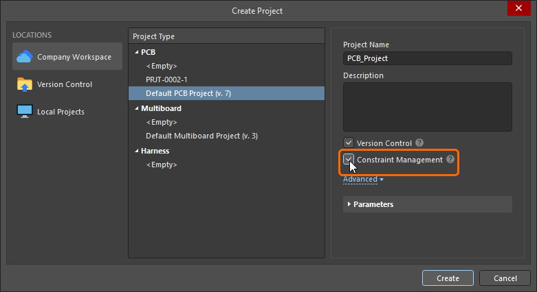 )。如果未启用,则必须使用 PCB Rule and Constraints Editor 。要快速检查当前 PCB 工程使用的是哪种设计约束管理方式,请打开该工程的 PCB 文档,单击 Design 菜单,并查看可用的是哪个命令:Constraint Manager – 本工程使用 Constraint Manager ,或 Rules – 本工程使用 PCB Rule and Constraints Editor 对话框。
本帮助页面展示了在 PCB Rule and Constraints Editor 对话框以及 Constraint Manager 中定义约束时的图示。请注意,术语 constraint 与 rule 可互换使用。
添加新的 Room Definition 设计约束
在 PCB Rules and Constraints Editor 中
对于每一个被放置或创建的 Room,都会自动创建一个关联的 Room Definition 设计约束。反过来也成立:如果你新增此类型的规则,对应的 room 对象也会出现在设计空间中。还要注意同样的反向关系:如果你在图形编辑器中删除一个 room,该约束会自动删除;或者如果你删除该设计约束,则图形对象也会被删除。
如果从 PCB Rules and Constraint Editor 定义 room 约束,则会创建一个默认 5 英寸 × 5 英寸的 room 对象,位置在 Absolute Origin(编辑空间左下角)向内 1 英寸处。请注意,原点标记显示的是用户定义的 Relative Origin,它可以设置在编辑空间的任意位置。
 添加新的 room 约束时,会在编辑空间中定义一个默认 room。
添加约束后,你可以返回编辑空间并 以图形方式编辑 room。或者,当你在 PCB Rules and Constraints Editor 中时,也可以编辑 room 约束,然后单击 Define 按钮以交互方式定义形状。 由于 room 定义的是板上的一个区域,更常见的做法是交互式放置 room,并让系统自动创建相应的设计约束。
了解更多关于如何在 PCB Rules and Constraints Editor 中添加新约束的信息。
在 Constraint Manager 中
要在 Constraint Manager: 中创建新的限制(room)约束,请切换到 All Rules 视图,在 Placement 类别中选择 Room Definition,然后在 Advanced Rules 列表中右键单击,并从右键菜单中选择 Add Advanced Rule,如下所示。
 可在 Constraint Manager 中添加新的 room 约束。
此时,图形编辑空间中还不存在 room 对象;你必须单击 Define 按钮(会切换到 PCB 编辑器)并定义 room 的形状。完成后,room 约束与 room 对象都会存在,并且可以保存这些约束。
-
如果 room 约束将用于限制对象必须位于该板区域内部(或外部),下一步是在 Constraint Manager 底部配置 Object Match 以及其他约束设置。继续阅读以了解更多内容。
-
如果 room 约束将作为另一类约束(例如布线宽度)的区域定义,请参阅 Defining Constraints Within a Room 小节了解更多。
了解更多关于如何在 Constraints Manager 中添加新约束的信息。
什么是 Room 约束?
如前所述,room 是 PCB 某个表面层上的一个已定义区域,用于在该板区域内定义设计要求。
所有设计约束都有两个关键要素:
-
what objects this constraint applies to(
 ),以及,
),以及,
-
how those objects are to be constrained(
 )。
)。
如果 room 约束定义在板上没有任何元件的区域,则 Object Match 条件(the objects this constraint applies to)默认会是 False,这意味着该约束不适用于任何对象。请按需编辑。
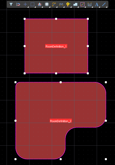
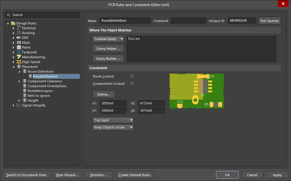 新创建的 room 定义。注意规则作用域为 False,表示它不适用于任何对象。
约束一个元件类
room 约束的一种常见用法是定义某个元件类的位置,将该类元件锁定在板上的特定区域内。
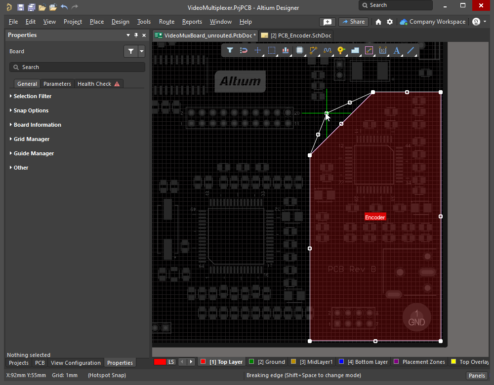
 Encoder 元件类被约束在名为 Room-Encoder 的 room 内,位于板的 Top Layer。
上图展示了在 PCB Rules and Constraints Editor 中(本质上与 Constraint Manager 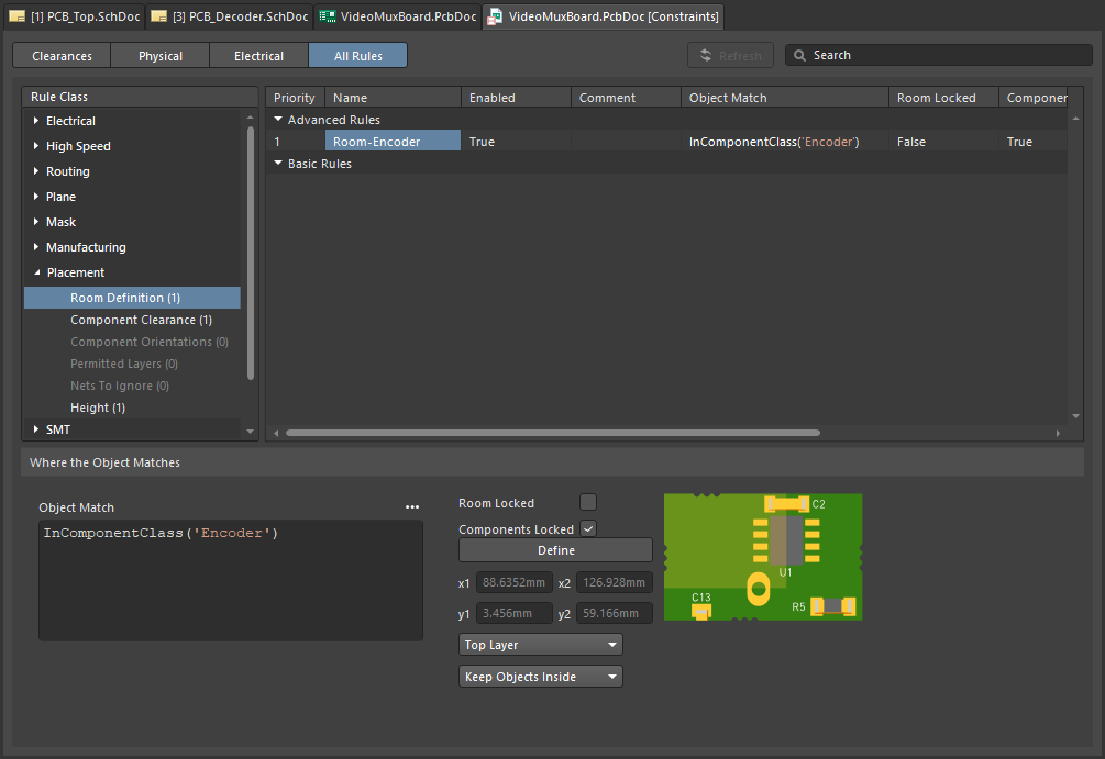 相同),
相同),Encoder 元件类如何被约束 within Room-Encoder room 内,并位于板的 Top side 上。 一旦元件被分配到某个 room,当 room 移动时它们也会随之移动。若要移动 room 而不移动元件,请临时禁用关联的 Room Definition 规则。
了解更多关于 Room Definition 设计约束 的信息。
PCB 编辑器包含多种用于处理 room 的强大工具,更多内容请阅读本页的 Working with Rooms 小节。
除了作为独立的设计约束(Room Definition)之外,room 还可以作为对象,用于将另一项设计约束的作用域聚焦到板上的某个区域,例如 Width、Clearance 或 Via Style。本主题在本页的 Defining Constraints Within a Room 小节中讨论。
Created During Schematic to PCB Design Synchronization
当设计从原理图传输到 PCB 时,你可以选择为每张原理图页上的元件创建一个 room。在多层级的层次化设计中这可能价值不大,但在大型扁平化设计中,为每张 sheet 设置一个 room 在板上摆放元件时会很有帮助。
Project Options dialog 的 Class Generation tab 包含用于为设计中的每张 sheet 生成 room 的选项 (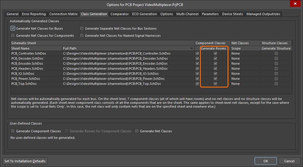 )。如果勾选 Generate Rooms 选项,则在运行 Design » Update 命令时,会为该 sheet 创建一个 room,并将该 sheet 内所有元件组成的一个类分配到该 room。请注意,每张 sheet 中的元件都会被加入到一个元件类中,因此 Generate Rooms 选项还要求同时启用相应的 Component Class 选项。
在 PCB 中,每个 room 约束都会以 InComponentClass('<SheetSymbolDesignator>') 作为作用域创建。如果某张 sheet 不包含任何元件,则不会创建 room。初次将原理图传输到 PCB 时,每个元件类中的元件会被排列成一行,然后围绕该元件类创建一个 room,如下图所示。
如果不需要自动生成的 room,请在 Project Options dialog 中禁用 Generate Rooms 复选框。
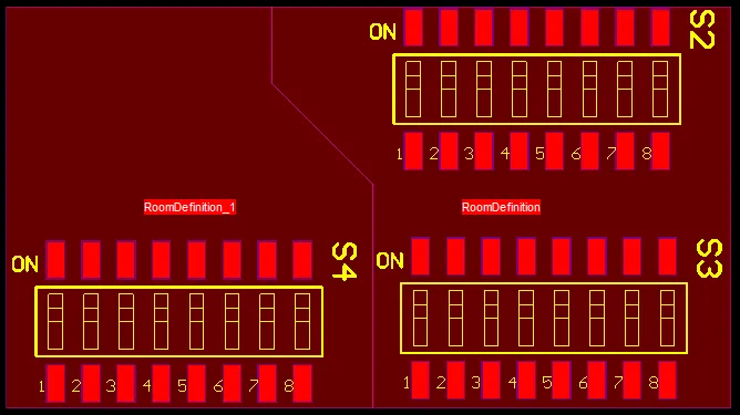
 初次设计同步后的 PCB——为每张 sheet 创建了一个 room,并将该 sheet 的元件类分配给它。
了解更多关于从原理图工程自动生成 Rooms、Component Classes 和 Net Classes 的信息。
要了解更多关于设计同步的内容,请参阅 Keeping the Schematics & PCB Synchronized 页面。
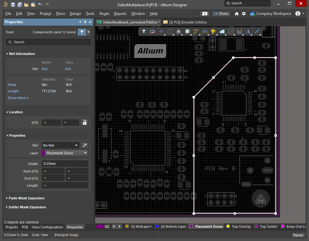
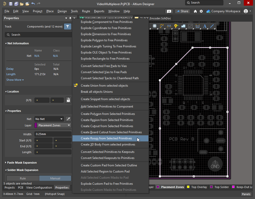
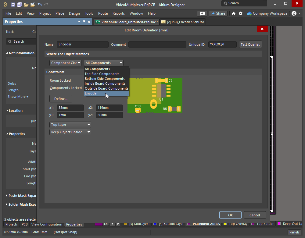
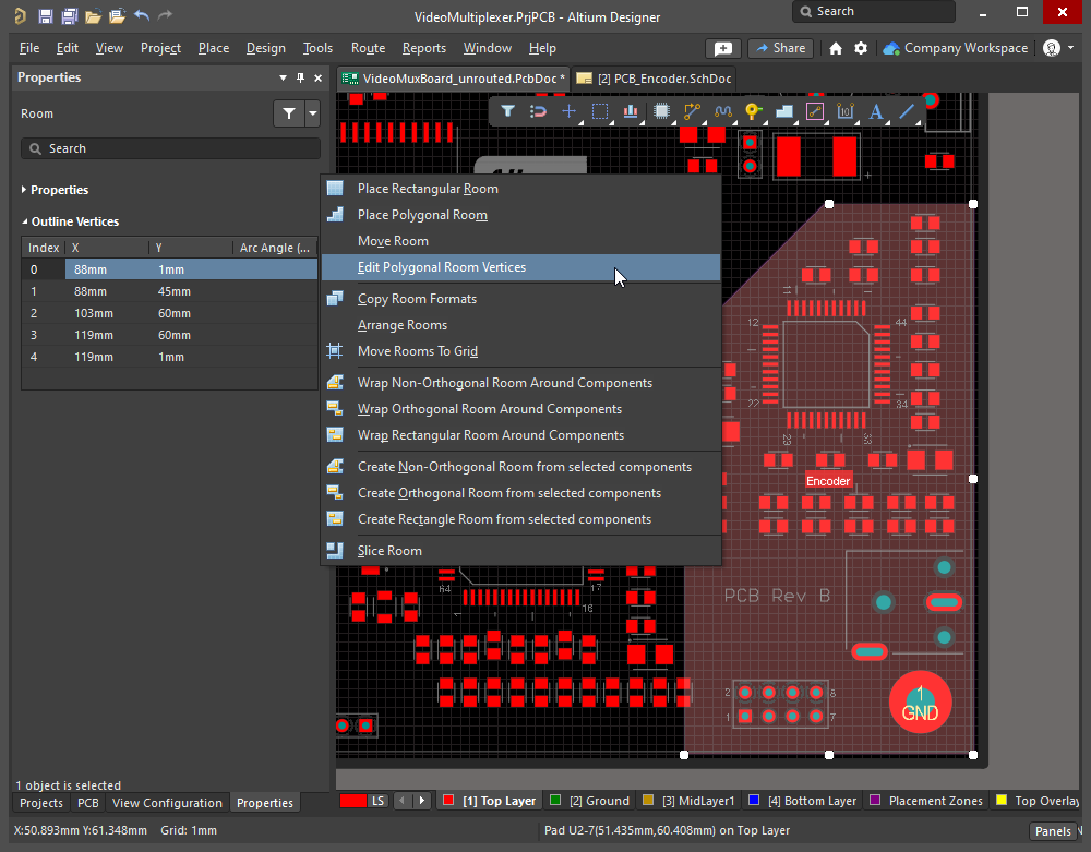
From Selected Tracks and Arcs
room 对象可以使用由所选 track 和/或 arc 对象组成的闭合边界来定义。为此,请在设计空间中选择该闭合边界的所有组成 track 与 arc 图元,然后从主菜单中选择 Tools » Convert » Create Room from Selected Primitives 命令。下面的幻灯片演示了相关步骤。
|
已在机械层上放置走线,用于定义编码器(Encoder)元件可用的板空间。 运行 Tools » Convert » Create Room from Selected Primitives 命令以创建相同形状的 Room Definition(房间定义)。 将出现 Edit Room Definition 对话框,以便定义该约束的参数。此房间将分配给 要调整房间的形状,单击选中它,然后运行 Design » Rooms » Edit Polygonal Verticies 命令, 并单击一个顶点或一条边来重新塑形房间。 |
编辑房间
可以交互式修改房间的 X-Y 形状以及其在板上的位置。请注意,用于交互式编辑房间有两种不同流程:一种基于其选择矩形(见 更改大小和位置 小节),另一种基于其形状编辑顶点(见 更改形状 小节)。
除了通过 Design » Rooms 子菜单访问命令外,你还可以在已放置的房间上右键单击并选择 Room Actions 子菜单,以访问与房间相关的上下文命令。
 在房间上右键单击以访问房间专用命令。
Changing the Size and Location
当你单击一次房间将其选中时,将出现以下编辑手柄——无论该房间最初是以矩形还是多边形方式放置:

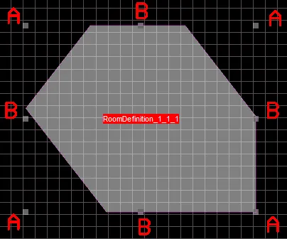 单击选中房间时会显示编辑手柄。
更改房间大小
-
拖动角点手柄(A)将同时在水平方向和垂直方向缩放房间。
-
拖动边缘手柄(B)将沿该方向缩放对象(水平或垂直)。
-
拖动时可通过按下以下按键旋转或镜像:
-
Spacebar 用于逆时针旋转对象,或 Shift+Spacebar 用于顺时针旋转。旋转步进遵循 PCB Editor - General page 中定义的 Rotation Step 值,该页面位于 Preferences 对话框内。
-
X 或 Y 键用于沿 X 轴或 Y 轴镜像对象。
-
L 键用于将对象翻转到电路板的另一面。如果房间关联了元件,这些元件也会随房间一起翻转。
-
移动房间
在房间上单击并拖动即可将其移动到新位置。 也可以通过主菜单中的 Design » Rooms » Move Room 命令或房间右键菜单中的 Room Actions » Move Room 命令来移动房间对象。 启动命令后,光标将变为十字准星,你将进入房间移动模式——单击房间以移动它。
当你单击房间以移动它时:
-
房间将吸附到光标上。房间被“抓取”的点取决于当前的 Object Snap Options(
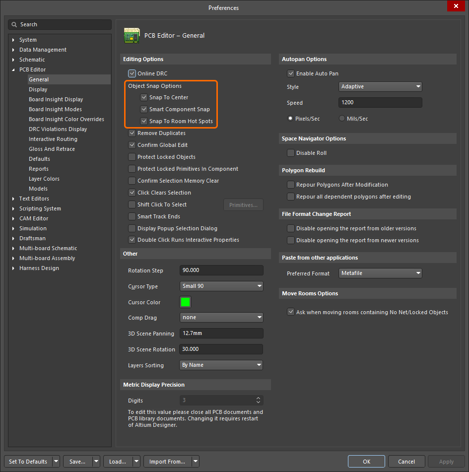 ),光标会吸附到已启用吸附点中最近的一个(元件焊盘、元件标号或房间顶点)。
-
将房间移动到所需位置,然后单击或按 Enter 以完成放置。
-
继续移动更多房间,或右键单击/按 Esc 退出。
-
如果被移动的房间中包含元件,可在移动过程中按 Shift 或 Ctrl 键显示绿色动态对齐引导线。使用 Shift 保持吸附到活动栅格,使用 Ctrl 临时抑制栅格并对齐到现有的非栅格对象。
-
如果房间包含任何 No Net 对象和/或锁定对象,将打开 Room containing No Net/Locked Objects 对话框。使用该对话框确定这些对象是否应随房间一起移动,然后单击 OK。 要使该对话框出现,必须在 Preferences 对话框(
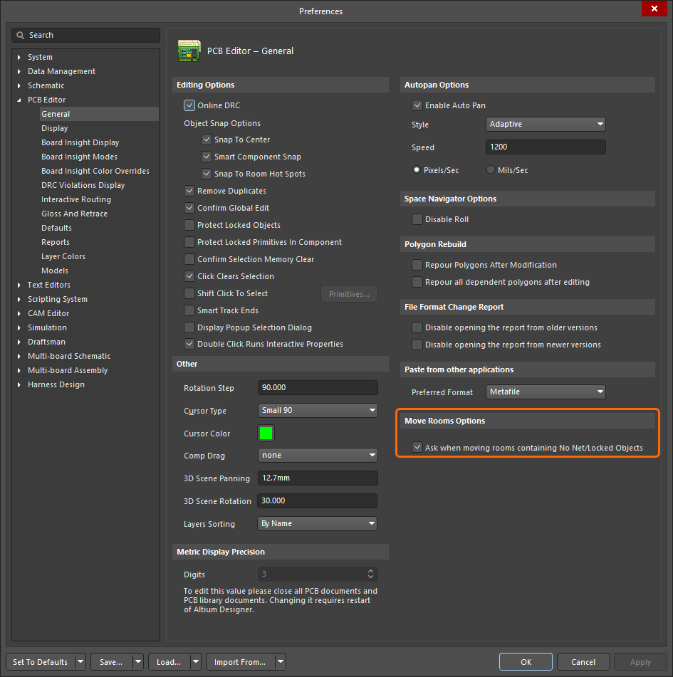 )的 PCB Editor - General 页面启用 Ask when moving rooms containing No Net/Locked Objects 选项。

Room containing No Net / Locked Objects 对话框
包含 No Net / 锁定对象的房间对话框 |
|
| No Net Objects | 启用后,将无网络(no nets)的对象随房间一起移动。 |
| Locked Objects | 启用后,将锁定对象随房间一起移动。 |
| Don't ask me about moving room's locked/no net objects until next PCB session (use currently selected settings) | 启用此选项可保存所选设置,并在本次 PCB 会话的其余时间继续使用。该对话框在新会话开始前不会再次打开。 |
Changing the Shape
通过运行 Edit Polygonal Room Vertices 命令来修改房间的边界形状。该命令可通过 Design » Rooms 子菜单访问,或通过右键 Room Actions 上下文子菜单访问。
运行该命令后,将显示房间多边形边界形状的边界编辑手柄,然后你可以:
-
单击一个 A 手柄,然后移动光标以移动该顶点。再次单击新位置以放置该顶点。
-
移动 A 手柄时,按键盘上的 Delete 键可从房间中移除该顶点。
-
单击 B 或在一条边上单击(手柄之间),然后移动光标以滑动该边。移动边时按 Shift+Spacebar 可在可用的 边行为模式(滑动边、断开边、弯曲边)之间循环切换。
-
Ctrl+Click B在一条边上单击 Ctrl+Click ,然后移动光标以在该边上添加一个顶点并同时移动该顶点。再次单击新位置以放置该顶点。实际上,新顶点会成为一个 A 顶点,并且会在它与原始 A 顶点之间添加新的 B 顶点。
-
要访问非栅格上的手柄,按住 Ctrl 键可临时抑制栅格吸附。
-
按需继续修改房间形状,或右键单击/按 Esc 停止。房间显示将根据新的边界形状更新。
无论目标房间是否锁定,都可以使用此命令。
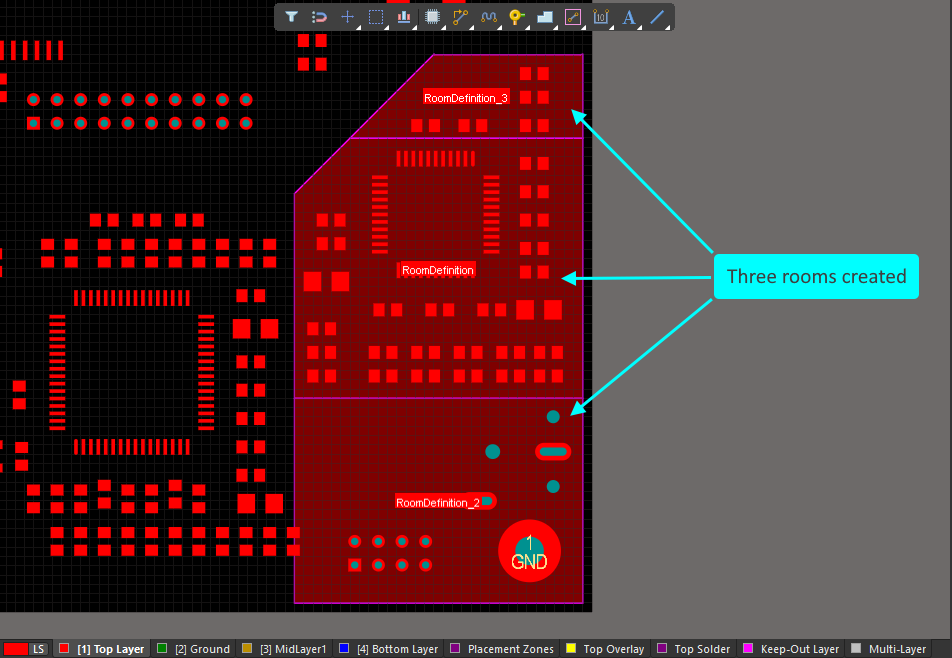
Slicing a Room
提供了一些命令,可通过图形方式将已放置的房间对象slice切分为两个或多个独立房间。切分过程类似于放置一条线,并包含相同的拐角模式(实际上,切分对象的宽度就是当前默认线宽)。请注意,用于显示切分路径的对象并不是正在放置的对象,它们仅用于显示切分路径,并会在切分过程完成后被移除。此外,无需从房间边缘精确开始切分;更容易的做法是从房间外稍微开始,并在房间外稍微结束。
有两条可用的切片命令。两者在定义切片路径的流程上相同,不同之处在于它们如何处理被切片房间(Room)中已有的元件。在描述完切片流程后,将解释这两条命令之间的差异。
|
在房间上单击右键,可在Slice菜单中访问Room Actions命令。 使用下文所述流程定义了两条切片。 已创建三个房间。 |
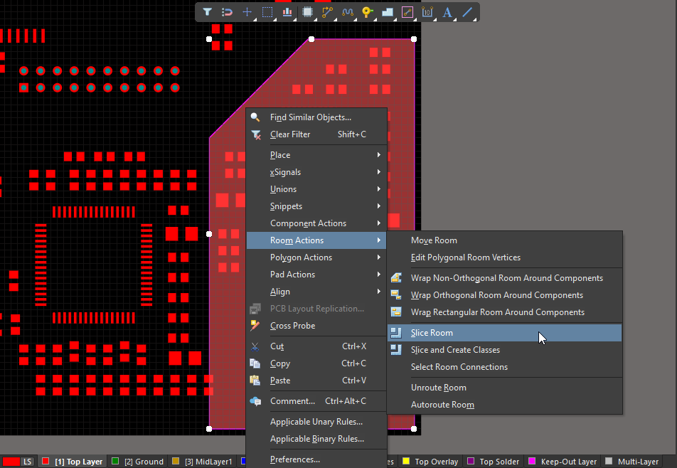
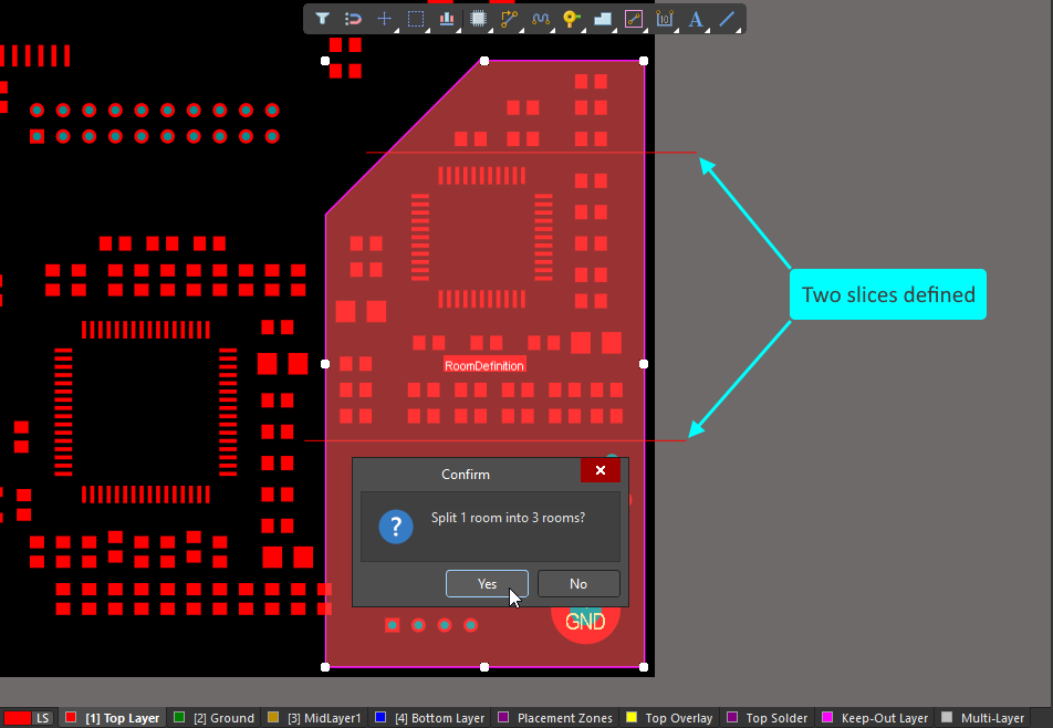
切片流程
启动Slice命令后:
-
光标会变为十字准星,并提示你选择切片的起点。
-
将光标放在要切片的房间外侧一点,然后单击或按Enter。此时进入切片模式(本质上是放置线段的模式)。
-
将光标移入房间以定义第一条切片边,然后单击或按Enter以锚定该边的终点。
-
继续移动光标并单击,定义一系列顶点,从而确定切片的形状。
-
放置最后一个顶点(位于房间外侧一点)后,单击右键或按Esc 以完成该切片的放置。
-
现在你可以继续对该房间开始另一条切片, 或单击右键/按Esc 退出切片模式。
-
将打开确认对话框,说明原始房间将被分割成多少个房间。单击Yes以提交你所做的切片,或单击No 以丢弃。生成的新房间对象将相应更新,并创建并关联相关的 Room Definition 规则。
-
切片过程中,按:
-
Shift+Spacebar以循环切换拐角模式。
-
Spacebar以切换拐角方向。
-
每条切片边都需要一个起点和终点。
-
如果切片放置模式包含拐角,按 1 快捷键可在“每次单击放置一条边”和“每次单击放置两条边”之间切换。
-
Backspace以移除最后放置的切片边。
-
Editing in the Properties Panel
房间对象比较特殊,因为它既是一个对象,也是一个设计约束。
通过 Properties 面板编辑
当选中房间时,可在Properties面板中编辑房间对象的属性,包括其在编辑空间中的位置与形状。可通过设计空间右下角的 Panels Panels按钮显示该面板,或使用 View » Panels » Properties命令。
 Properties面板可用于编辑房间的图形属性。
| Name | 房间的当前名称(以及关联的 Room Definition 规则)。可按需更改。名称不仅有助于识别每个房间,还可用于在设计规则中定位特定房间。 |
| (X/Y)(两个字段) | 房间第一个顶点相对于当前原点的 X 与 Y 位置。编辑字段中的数值可改变房间相对于当前原点的位置。数值可用公制或英制输入;当输入的单位不是当前默认单位时,请在数值中包含单位。默认单位(公制或英制)显示在状态栏上,并在Properties面板的Other区域中设置(当设计空间中未选中任何对象时)。只有在X/Y选项处于解锁状态(显示 |
Outline Vertices |
|
| Vertices Grid | 按房间放置时定义的顺序,列出当前为房间定义的所有顶点。使用直线边将一个顶点连接到下一个顶点。如果你希望使用圆弧连接,请为所需的 Arc Angle输入数值。数值输入在源顶点对应的字段中,圆弧将从该顶点连接到列表中其下方的下一个顶点。 单击右键可Copy / Paste或Import / Export to CSV。 |
| Index | 顶点的索引编号(不可编辑,基于房间定义时的放置顺序)。 |
| X | 该顶点的 X(水平)坐标。单击可编辑。 |
| Y | 该顶点的 Y(垂直)坐标。单击可编辑。 |
| Arc Angle (Neg = CW) | 用于将该顶点与下一个顶点连接的圆弧角度。默认连接为直线边,因此该字段保持为空。单击编辑并按需输入圆弧角度。输入正值将绘制逆时针圆弧;要绘制顺时针圆弧,请输入负值。 |
使用房间(Rooms)
软件包含多项功能,帮助你处理房间以及房间内的对象。这包括以下命令:将房间按网格模式排列;将房间移动到当前捕捉网格;以及对于包含重复电路段的设计,将一个房间的放置与布线复制到另一个房间。
你也可以使用房间将其他设计约束限制在电路板的某个区域内,例如要求在该房间内的网络必须以特定线宽与间距进行布线,或要求差分对必须以特定阻抗剖面进行布线。
 一个 8 通道混音器:先完成第一个输入通道的放置与布线,然后使用 Copy Room Format 命令将其复制到其余七个输入通道。
Defining Constraints Within a Room
除了将对象约束在房间内或房间外(如 Room Definition Design Constraint 一节所述)之外,房间还可以在其他设计约束中用作区域限制。例如,布线宽度约束可能要求 BGA 下方的布线使用不同的线宽,或者电气间隙约束可能要求在电路板的特定区域使用不同的间隙。
房间内的布线宽度和间隙会根据 Room Definition 中的设置自动调整。
这是通过添加下方幻灯片中所示的 Routing Width 约束和 Electrical Clearance 约束来实现的。
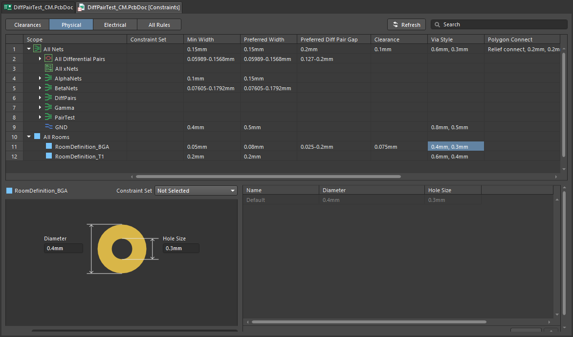
在 Constraint Manager 中
当在 All Rules 视图中添加房间约束时,该房间对象也会在 Physical 视图中可用。使用该视图,你可以快速定义必须在房间内应用的基于区域的约束,包括:布线宽度、电气间隙、过孔样式、差分对属性、布线颈缩(neck-down)以及多边形连接样式。下方幻灯片展示了上方视频中该电路板的约束。
|
在此房间内,所有布线对象的线宽必须在指定范围内。 在此房间内,所有布线对象与属于其他网络的对象之间必须至少保持这么大的间隙。 在此房间内,所有布线对象必须至少保持这么大的电气间隙。 在此房间内,所有差分对必须使用 |
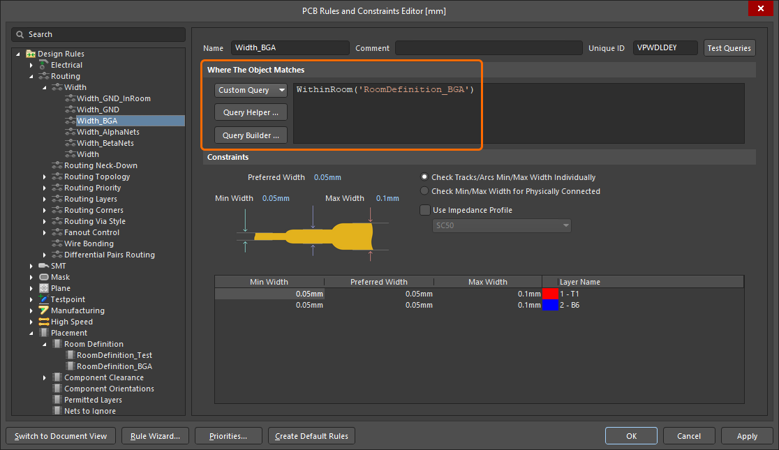
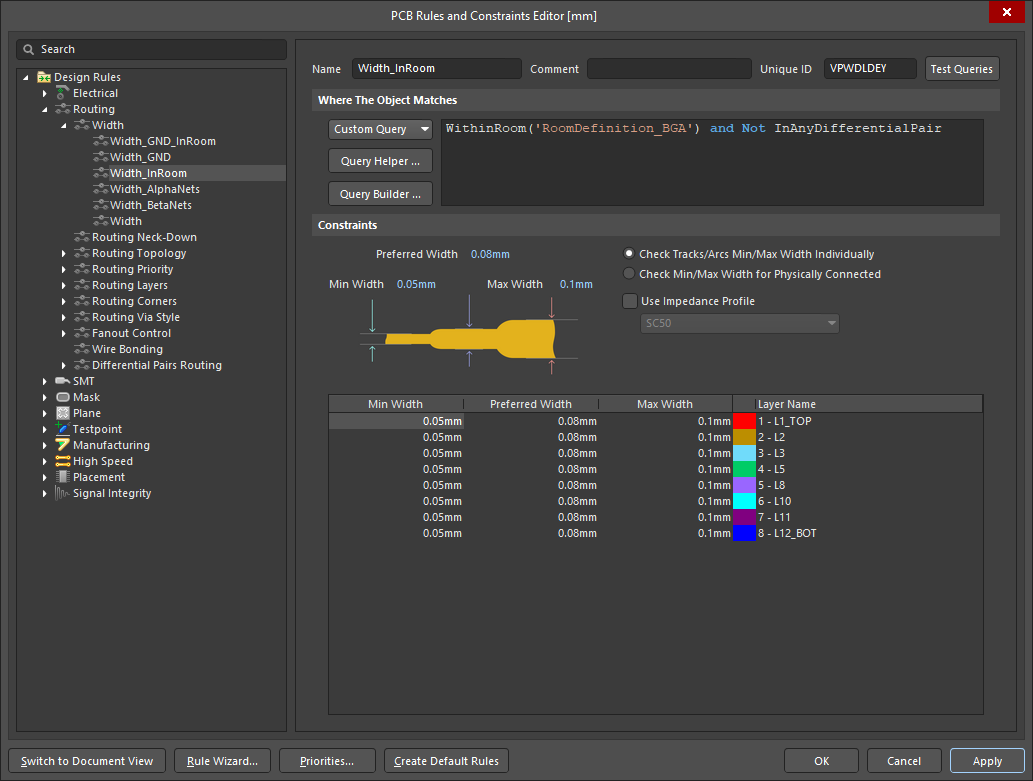
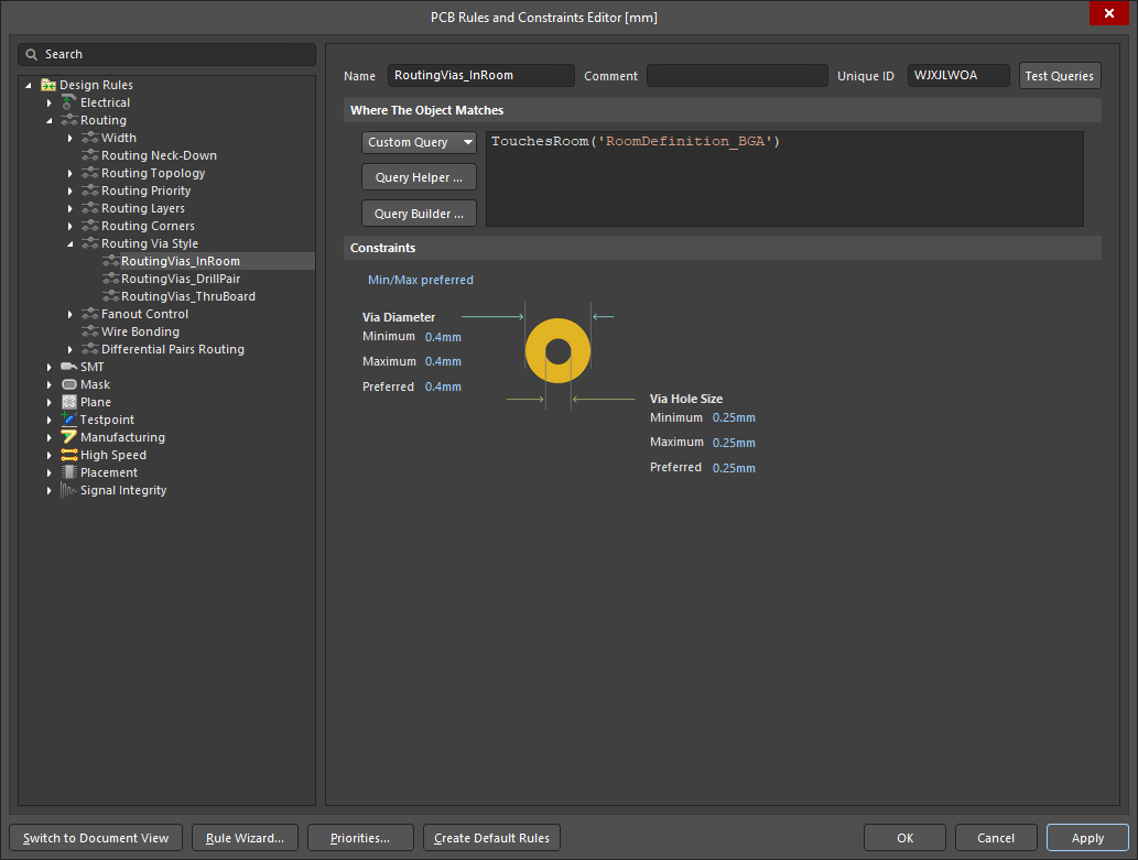
在 PCB Rules and Constraint Editor 中
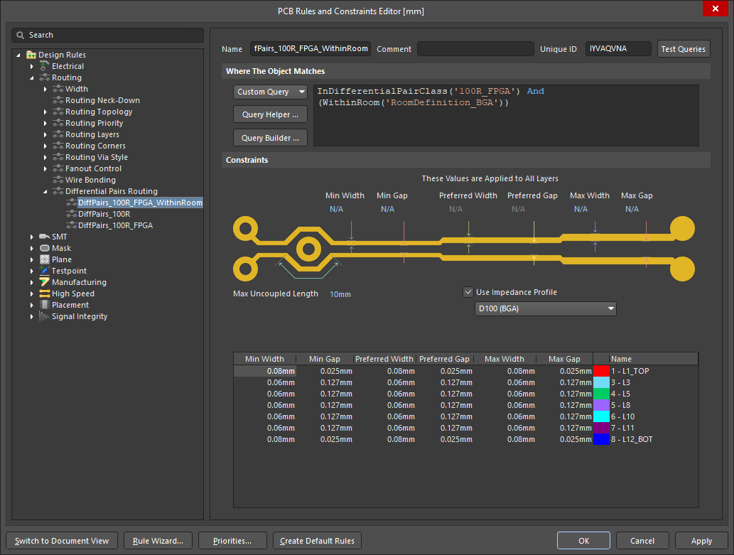
要在 PCB Rules and Constraint Editor 中实现相同结果,需要创建一个用于定义房间区域的查询。就房间内对象的检测方式而言,可以通过两种方式实现:针对完全落在房间内的对象(使用 WithinRoom 关键字),或针对与房间接触的对象(使用 TouchesRoom 关键字)。下方幻灯片演示了与前一个 Constraint Manager slideshow 中相同的布线宽度、电气间隙、过孔样式以及差分对属性。
Arranging Selected Rooms
要在设计空间内排列所选房间,可以使用 Design » Rooms » Arrange Rooms 命令。选择所需房间,然后启动该命令以打开 Arrange Rooms 对话框。
 Arrange Rooms 对话框。
指定你希望如何排列房间,以及它们的放置顺序。你还可以指定起始位置——可在对话框中输入 X-Y 坐标,或在工作区中单击——以及相邻房间之间的间距。单击 OK 后,所选房间将被移动到位。
Columns/Rows |
|
| Columns | 用于放置房间的列数。按需编辑此字段。 |
| Rows | 用于放置房间的行数。按需编辑此字段。如果房间数量超过自定义行列排列所能容纳的数量,将在顶部添加更多行。 |
Sort By |
|
| SortBy | 显示所选排序方式,即用于区分第一个房间与下一个房间的条件。可用选项详见下文。 |
| Channel Name | 按通道名称对房间进行字母数字排序。了解更多关于多通道设计的信息。 |
| Room Area | 按房间面积对房间排序。 |
| Room Component Count | 按房间包含的元件数量对房间排序。 |
| Room Width | 按房间的 X(水平)尺寸对房间排序。 |
| Room Height | 按房间的 Y(垂直)尺寸对房间排序。 |
| Sort in Ascending order | 启用后,将根据当前 SortBy 条件按升序(从小到大)排序房间。若禁用此选项,则为降序(从大到小)。 |
Position |
|
| Origin X | 定义开始放置房间的 X(水平)位置。编辑此字段以更改 X 坐标,可使用 mm 或 mil 单位。输入数值时如需指定单位,请在数值后添加 mm 或 mil 后缀。 默认单位(公制或英制)由 Units 设置在 Properties panel 中决定;若未指定单位,则使用默认单位。 |
| Origin Y | 定义开始放置房间的 Y(垂直)位置。编辑此字段以更改 Y 坐标,可使用 mm 或 mil 单位。输入数值时如需指定单位,请在数值后添加 mm 或 mil 后缀。 默认单位(公制或英制)由 Units 设置在 Properties panel 中决定;若未指定单位,则使用默认单位。 |
| Select Origin Using Mouse | 启用后,将提示你手动设置房间排列的原点。必须禁用 选项才能编辑 Origin X 和 Origin Y。 |
| X-Spacing | 定义相邻房间之间保留的 X(水平)距离。 |
| Y-Spacing | 定义相邻房间之间保留的 Y(垂直)距离。 |
| Auto Spacing | 启用后,房间将以相同的 X(水平)与 Y(垂直)间距进行排列。必须禁用 选项才能编辑 X-Spacing 和 Y-Spacing。 |
| Place On Grid | 启用后,强制房间排列与当前 PCB 捕捉网格对齐。 |
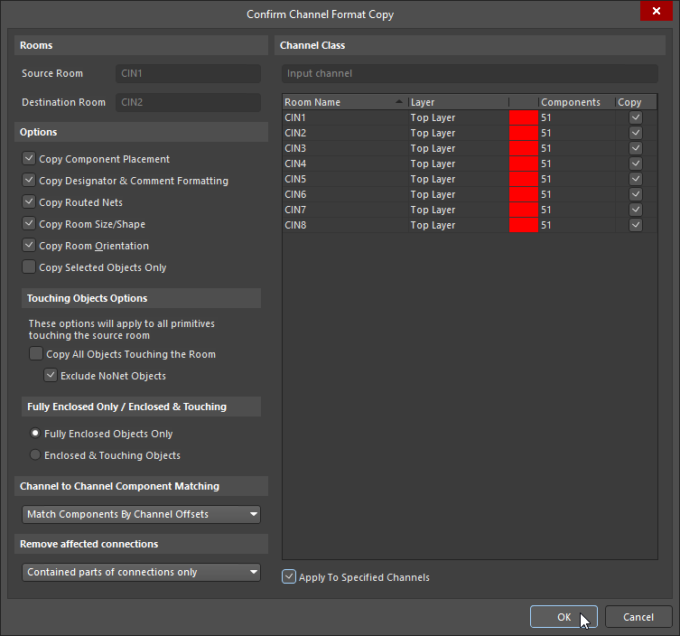
Copying Room Formats
房间最强大的功能之一,是能够将某个房间的房间形状、放置和布线复制到其他包含相同元件集合的房间中。该命令在多通道设计的布局过程中尤其有用,可将一个通道中完成的放置与布线传播到所有其他通道。
要将一个房间的格式复制到其他房间:
-
在主菜单中单击 Design » Rooms » Copy Room Formats。
-
状态栏会提示选择源房间。将光标移到源房间上方并单击,或按 Enter。
-
状态栏会提示选择目标房间。将光标移到你希望复制格式到的房间上方并单击,或按 Enter。如果你打算将格式应用到多个房间,则第二次单击可以在任意一个房间上进行。
-
Confirm Channel Format Copy 对话框将打开。使用这些选项定义所需的格式复制内容。格式复制默认从所选 Source Room 应用到所选 Destination Room。要从源房间复制到检测到的 Channel Class 中的每个房间,请启用 Apply to Specified Channels 选项,并确认目标房间所需的 Copy 复选框已启用。
-
在对话框中单击 OK 以更新目标房间。
-
你可以继续选择其他 目标 房间,或右键单击结束。
Rooms |
|
| Source Room | 源房间的名称(代表原理图中的通道),其元件放置与布线将被复制。 |
| Destination Room |
|
 )。请注意:如果要将某个源通道(房间)的格式复制到其他通道(房间),源通道(房间)与目标通道(房间)必须属于同一个通道类。
选项
接触对象选项
仅完全包围 / 包围并接触
通道到通道器件匹配
移除受影响的连接
Channel Class
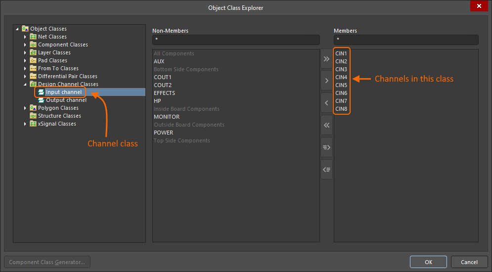
当多通道设计从原理图传递到 PCB 时,重复电路(通道)会在 PCB 编辑器的 Object Class Explorer 对话框(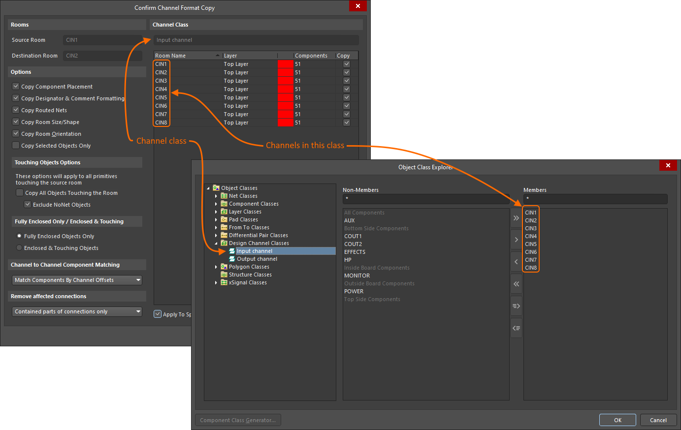 )中被识别为一个 Channel Class。正是该 Channel Class 用于确定格式复制要应用到哪些通道。 如果对话框的 Channel Class 区域为空,请检查是否已在 Object Class Explorer 对话框(Design » Classes)中正确定义 Channel Class。若未识别到任何 Channel Class,则复制命令仅从 Source Room 应用到 Designation Room。
Hiding Rooms
可通过 View Configuration 面板的 View Options 选项卡上的选项,对当前文档中的 Rooms 进行全局显示、隐藏或以草稿模式显示。
 调整 Rooms 的对象可见性滑块,使其在编辑区域中淡化或隐藏。
 AI 翻译
AI 翻译