Working with the Minimum Solder Mask Sliver Design Rule on a PCB in Altium Designer
Rule category: Manufacturing
Rule classification: Binary
Summary
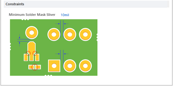
This rule helps identify narrow sections of solder mask that may cause manufacturing problems at a later stage. Ensuring that there is a minimum width of solder mask across the board, this rule checks the distance between any two solder mask openings that are equal to or greater than a user-specified value. This includes the pads, vias, and any primitives that reside on solder mask layers. It also checks Top and Bottom sides independently.
Constraints

Default constraint for the Minimum Solder Mask Sliver rule.
- Minimum Solder Mask Sliver - specifies the minimum allowed width of solder mask.
How Duplicate Rule Contentions are Resolved
All rules are resolved by the priority setting. The system goes through the rules from highest to lowest priority and picks the first one whose scope expressions match the object(s) being checked.
Rule Application
Online DRC and Batch DRC.
