Working with the SMD To Plane Design Rule on a PCB in Altium Designer
Created: 三月 22, 2017 | Updated: 九月 26, 2019
| Applies to versions: 18.0, 18.1, 19.0, 19.1, 20.0, 20.1 and 20.2
您正在阅读的是 20.0. 版本。关于最新版本,请前往 Working with the SMD To Plane Design Rule on a PCB in Altium Designer 阅读 21 版本
Rule category: SMT
Rule classification: Unary
Summary
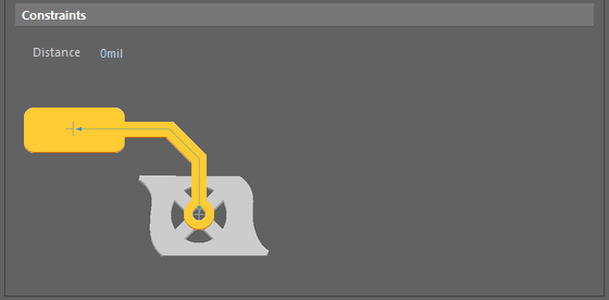
This rule specifies the maximum routing length from the center of a surface mount pad to the center of the pad/via connecting to a power plane.
Constraints
 Default constraints for the SMD To Plane rule.
- Distance - the value for the maximum permissible distance from SMD pad to pad/via connecting to the power plane.
How Duplicate Rule Contentions are Resolved
All rules are resolved by the priority setting. The system goes through the rules from highest to lowest priority and picks the first one whose scope expression matches the object(s) being checked.
Rule Application
Online DRC and Batch DRC.
