
KB: 3D Layout Mode Shows Excess Material Removal When Using Route Tool Path Layer
 Altium Designer
Solution Details
Symptoms of size mismatch between 2D and 3D
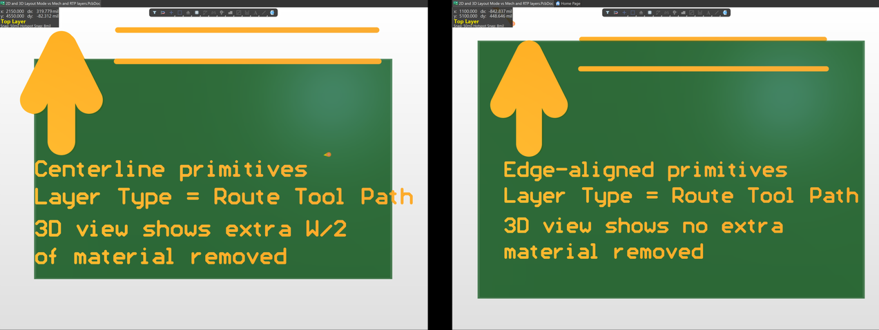
A PCB may appear correct in 2D Layout Mode but smaller in 3D Layout Mode.
- The board outline appears wider in 2D.
- The 3D model shows material removed along the board edge.
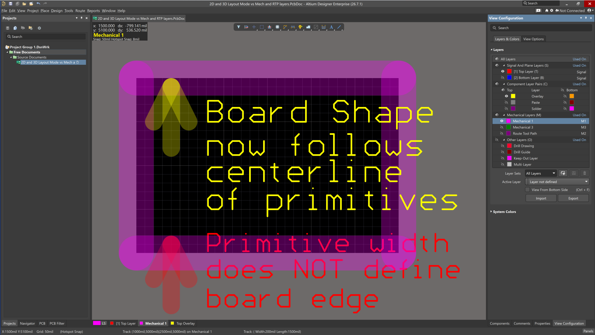
- The discrepancy typically equals half the primitive width.
This behaviour occurs when primitives used to define the board outline are placed on the Route Tool Path layer instead of a mechanical or Keep-Out layer.
Root cause of centerline versus edge interpretation
The difference is caused by how primitives are interpreted in each mode and their intended function:
- Board Shape definition is based on the centerline of selected line/arc primitives.
- Route Tool Path represents the physical machining path used during PCB fabrication.
- In 3D Layout Mode, the system removes material according to the full width of Route Tool Path primitives.
- No centerline compensation is applied when rendering material removal.
If primitives are centered on the board edge, half of their width extends into the board area, resulting in unintended material removal equal to half the primitive width. This behaviour is expected functionality and reflects how the Route Tool Path layer models real-world routing operations.
Recommended usage and design decisions
- ✅ Define the board outline using a mechanical layer or the Keep-Out layer.
- ✅ Use Design » Board Shape » Define Board Shape from Selected Objects for outline creation.
- ✅ Generate Route Tool Path primitives from the board shape using the dedicated command.
- ❌ Do not use the Route Tool Path layer to define the board outline.
Incorrect use of the Route Tool Path layer can lead to:
- Misinterpretation of PCB dimensions
- Incorrect fabrication assumptions
- Inconsistent 2D versus 3D visual results
Step-by-step workflow for correct implementation
- Place line/arc primitives forming a closed boundary on a mechanical or Keep-Out layer.
- Select the primitives.
- Run Design » Board Shape » Define Board Shape from Selected Objects.
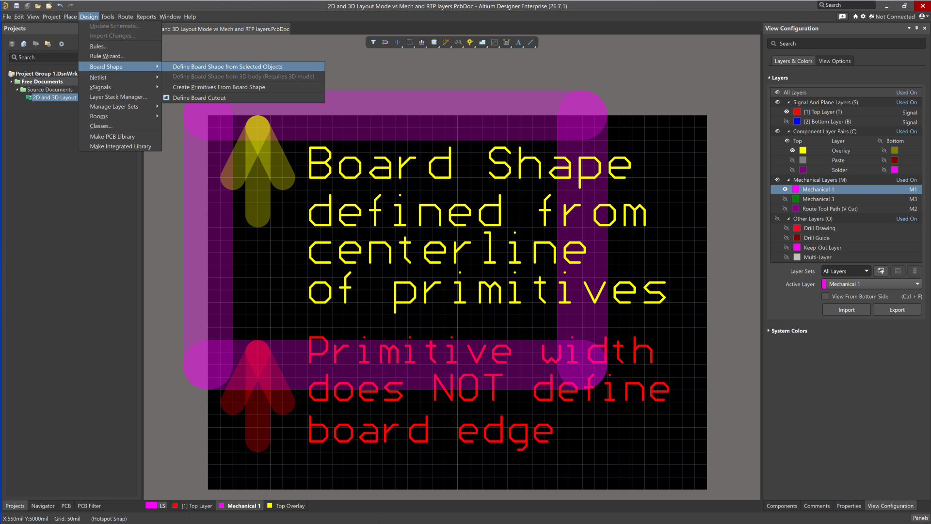
- Verify the board shape in 2D Layout Mode.
- Run Design » Board Shape » Create Primitives From Board Shape.
- Enable the Route Tool Outline option in the dialog.
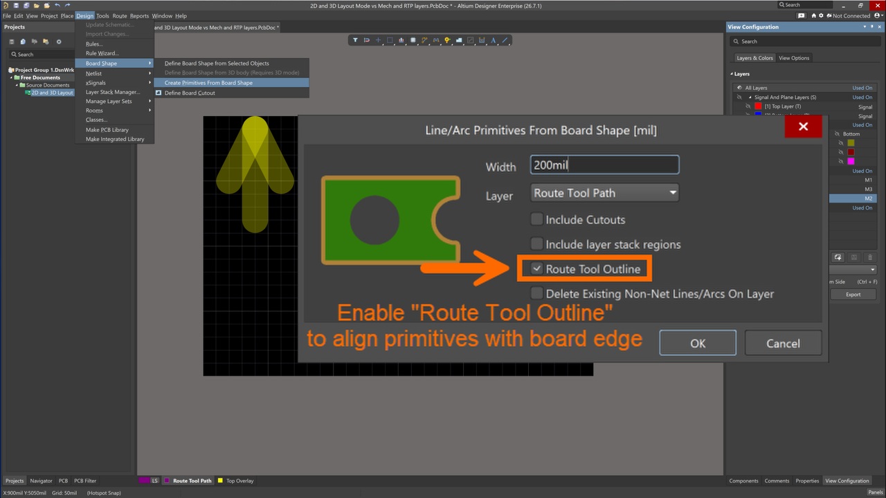
- Select a dedicated mechanical layer with Layer Type set to Route Tool Path.
- Generate the Route Tool Path primitives.
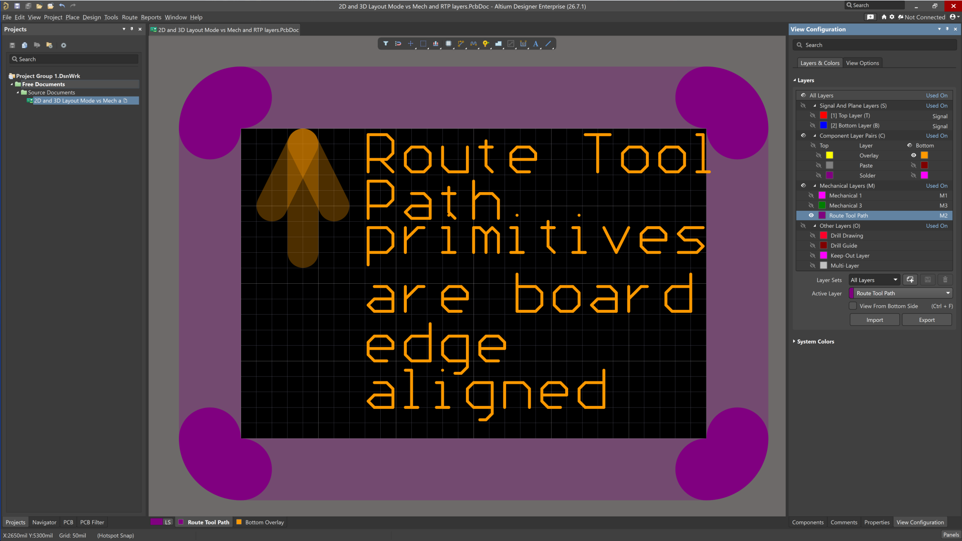
- Switch to 3D Layout Mode and confirm correct material removal.
For troubleshooting validation:
- Temporarily change the Route Tool Path layer type to a different layer type.
- Switch to 3D Layout Mode and confirm that excess material removal disappears.
- If resolved, recreate the Route Tool Path using the correct workflow above.
Additional Notes
The Route Tool Path layer is intended to represent the physical router bit path used during PCB fabrication. In 3D Layout Mode, this layer is used to simulate routed slots and material removal. It should not be used to define the board outline geometry.