Product 关闭

知识库:如何使用 SI Analyzer by Keysight 创建简单的传输线仿真

Altium Designer Altium Designer
本文介绍了在 Altium Designer 中使用 SI Analyzer by Keysight 创建简单传输线仿真的流程,旨在验证连接两个 SMA 连接器的传输线,其特性阻抗是否在规定的容差范围内达到目标值。该流程包括原理图绘制、PCB 布局、阻抗配置设置、约束定义和仿真分析。SI Analyzer 已集成到 Altium Designer 中,支持布局前和布局后的信号完整性分析。

解决方案详情

传输线阻抗验证场景与范围

目标是在两个 SMA 连接器之间设计一条具有指定长度和目标阻抗的传输线,并使用 Altium Designer 中的 SI Analyzer 验证其阻抗是否在可接受的容差范围内。

PCB 设计中阻抗失配的原因

高速 PCB 设计中的阻抗失配通常由走线宽度不正确、叠层定义不当或缺少约束定义引起。这些问题可能导致信号反射、信号劣化以及整体性能下降。如果未使用 SI Analyzer 等工具进行适当验证,这些问题可能直到设计周期后期才会被发现。

定义阻抗约束的可用方法

功能可用性:您可以使用的功能取决于您拥有的 Altium 解决方案 — Altium Develop、Altium Agile 的某个版本(Agile Teams 或 Agile Enterprise),或 Altium Designer(在有效订阅期内)。

仿真与验证的分步工作流程

  1. Create the project and schematic
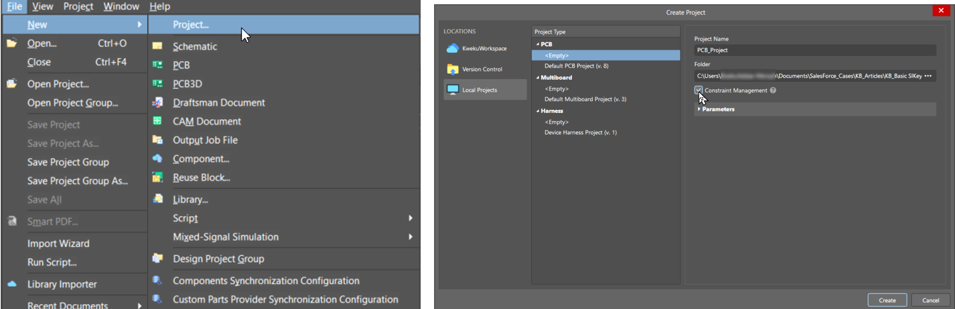
    • 在 Altium Designer 中新建一个项目。
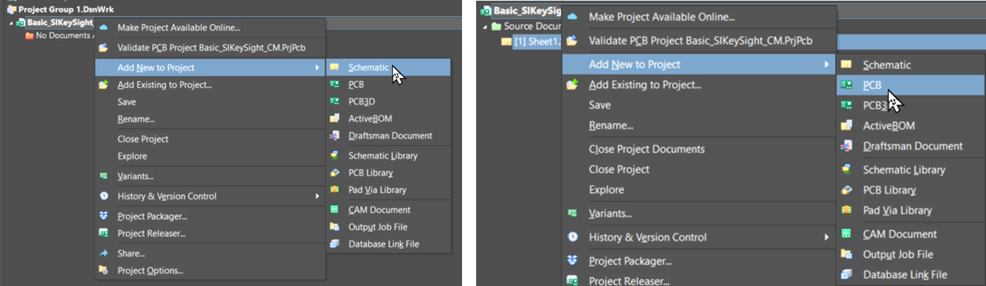
    • 添加并保存原理图(*.SchDoc)和 PCB(*.PcbDoc)文档。
    • 可选择在创建项目时启用约束管理。
      Altium Designer menus showing File > New > Project and the Create Project dialog, with PCB project type selected and the Constraint Management option enabled before creating the project.
      Altium Designer Projects panel showing right‑click menu on a PCB project with Add New to Project options, demonstrating adding a Schematic document versus adding a PCB document to the same project.
  2. Place SMA connectors
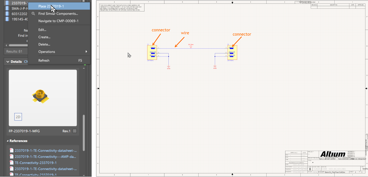
    • 从元件库(本地或 Altium 365 工作区)中选择 SMA 连接器。
    • 在原理图上放置两个连接器。
    • 使用导线连接信号引脚。
    • 将所有其他引脚连接到 GND。
      Altium Designer schematic editor showing two connector symbols connected by a wire on a single sheet, with ground symbols on each connector. Components panel at left lists a selected connector part with preview and references.
  3. Define impedance constraints
    • Design Directives Method:
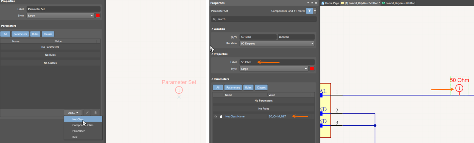
      • 为目标阻抗创建一个参数集。
      • 指定网络类名称,并将其与信号导线关联。
        Altium Designer schematic and Properties panels showing a Parameter Set placed on a signal. The Label reads “50 Ohm,” and the Net Class Name is set to 50_OHM_NET, applying an impedance rule to the connected net.  
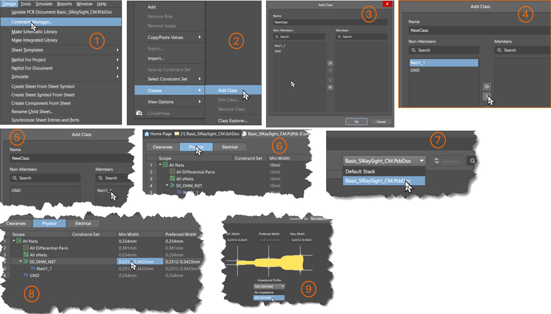
    • Constraint Manager Method:
      • 从原理图中打开 Constraint Manager。
      • 添加一个新类(例如 50OhmLine),并将目标网络分配给该类。
      • 在“物理”选项卡中设置首选宽度。
      • 在“走线宽度”窗口中选择阻抗配置。
        Altium Designer workflow collage showing creating a net class and assigning constraints: Design > Constraint Manager > Classes, adding Net1 and GND members, then setting clearance and impedance rules for 50_OHM_NET in PCB constraints.
        注意:必须先创建叠层和阻抗配置,才能完成此步骤。
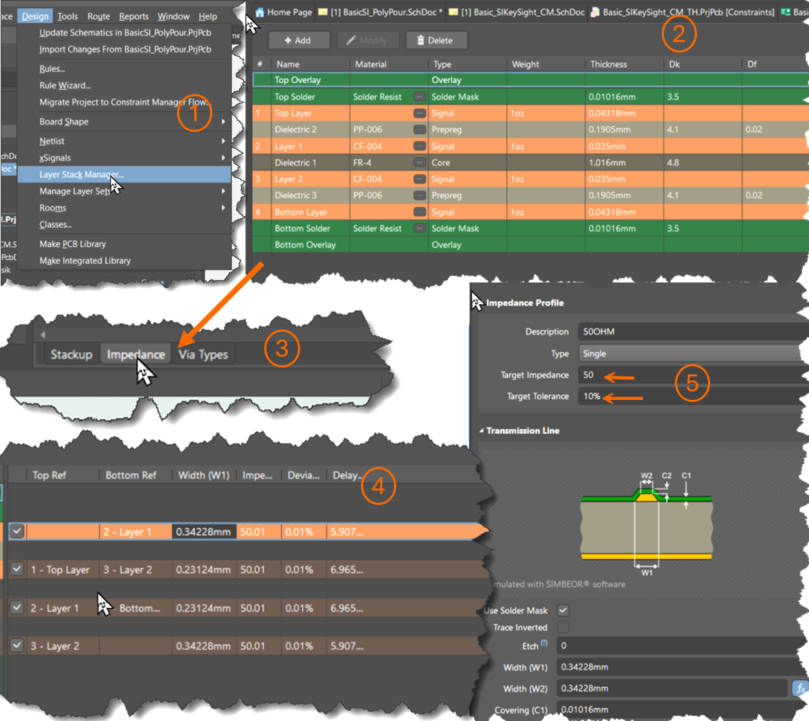
  4. Create stack-up and impedance profile
    • 在 *.PcbDoc 中使用适当的介电材料、厚度和铜重定义叠层。
    • 使用 Altium 的阻抗计算器或外部工具确定走线宽度。
      Altium Designer Constraint Manager showing layer stack and impedance setup. Stackup and Impedance tabs define a 50‑ohm single‑ended impedance profile, target tolerance 10%, with calculated trace widths mapped to signal layers.
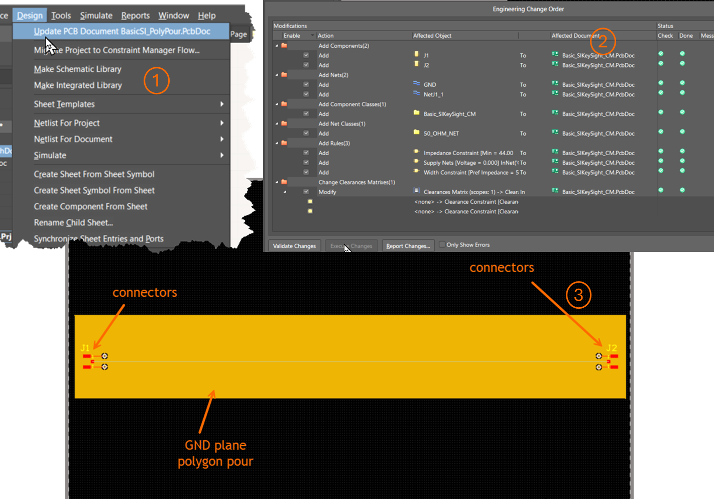
  5. Update PCB and complete layout
    • 使用 Generate ECO 更新 PCB。
    • 按所需间距在板框上放置连接器。
    • 将平面和多边形覆铜分配给 GND 网络。
      Altium Designer showing Design > Migrate Project to Constraint Manager Flow and an Engineering Change Order dialog with multiple applied changes, alongside a PCB view where two connectors are placed on a board with a GND plane polygon pour.
  6. Apply design rules and validate layout
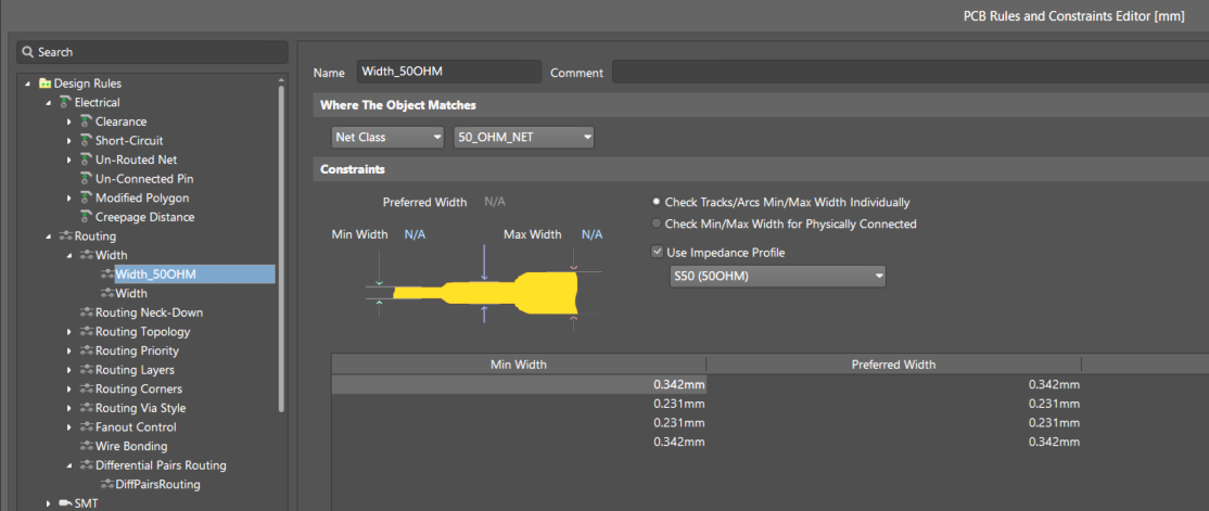
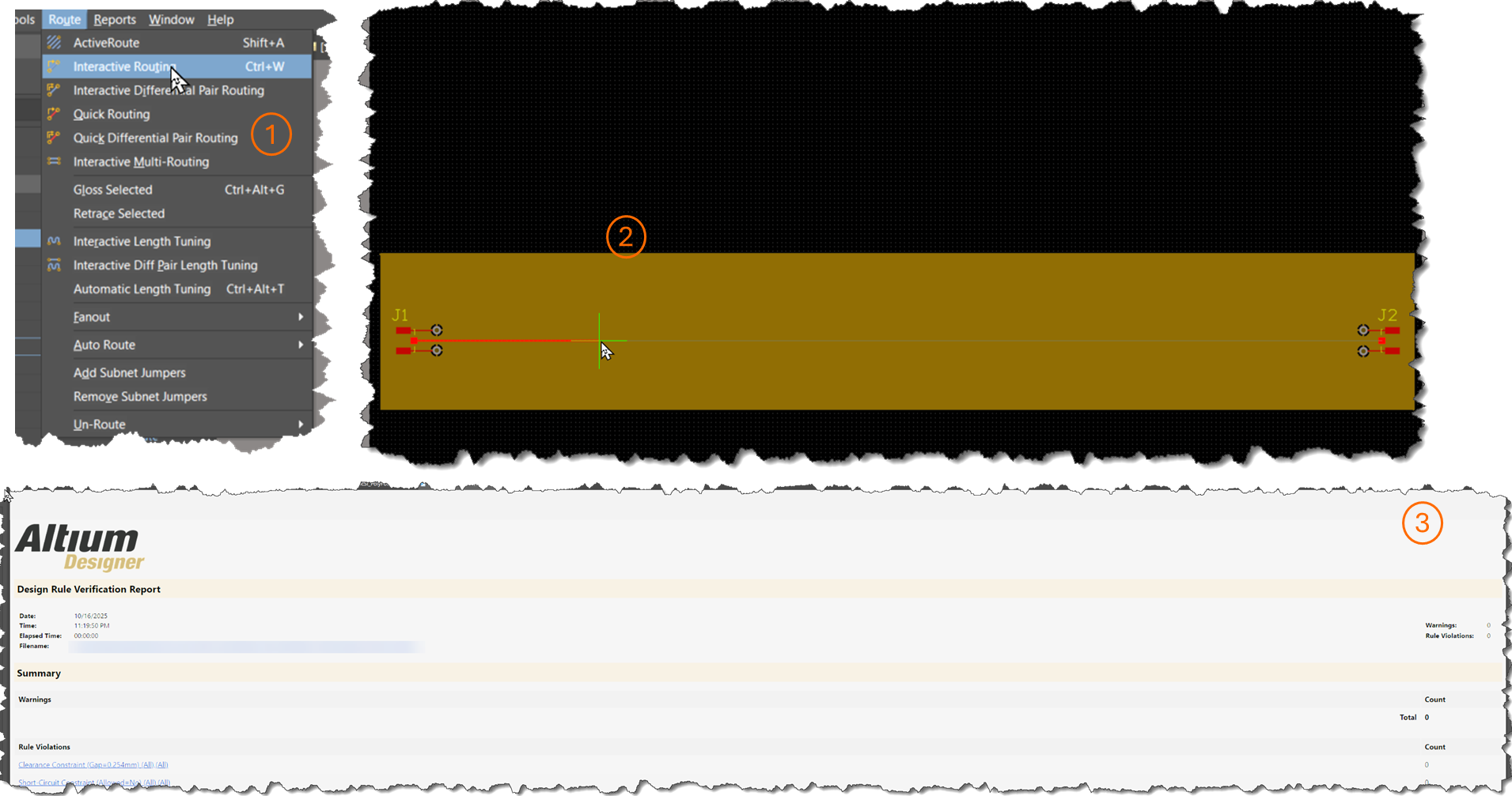
    • 使用阻抗配置或外部计算结果创建走线宽度设计规则。
    • Altium Designer 在交互式布线期间通过 PCB Rules and Constraints Editor 或 Constraint Manager 应用阻抗配置。
    • 适当连接接地焊盘和走线。
    • 运行 DRC 以检查错误。
      PCB Rules and Constraints Editor showing the Routing Width rule “Width_50OHM.” Scope targets Net Class 50_OHM_NET, with “Use Impedance Profile” enabled and profile S50 (50 OHM), defining calculated min and preferred trace widths per layer.
      PCB Rules and Constraints Editor showing the Routing Width rule “Width_50OHM.” Scope targets Net Class 50_OHM_NET, with “Use Impedance Profile” enabled and profile S50 (50 OHM), defining calculated min and preferred trace widths per layer.
  7. Run SI simulation and verify results
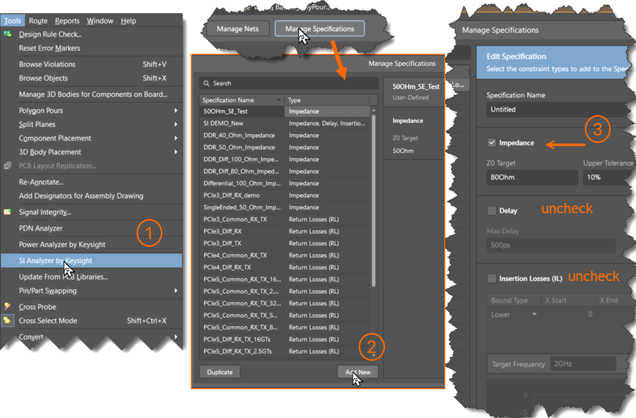
    • 加载集成在 Altium Designer 中的 SI Analyzer by Keysight。
    • 在 Manage Specifications 中创建阻抗规范(可跳过插入损耗、回波损耗和延迟)。
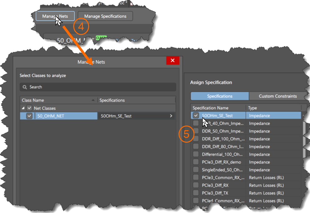
    • 在 Manage Nets 中,将该规范分配给目标网络或类。
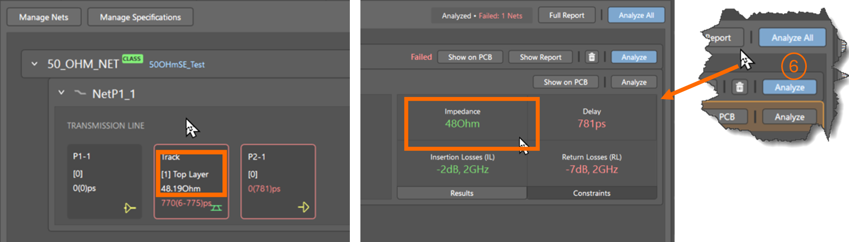
    • 单击 Analyze。
    • 确认阻抗在容差范围内满足目标值。
      Altium Designer SI Analyzer workflow showing Manage Specifications. A new user‑defined impedance specification is added with target impedance 50 ohm; Delay and Insertion Loss options are unchecked, focusing the spec on impedance only.
      Altium Designer SI Analyzer Manage Nets dialog showing Net Class 50_OHM_NET selected and assigned the impedance specification “50OHM_SE_Test,” linking the net class to a 50‑ohm single‑ended impedance analysis.
      Altium Designer SI Analyzer results view showing Net Class 50_OHM_NET analyzed and marked Failed. Transmission line summary reports impedance 48 ohm, delay 781 ps, and insertion and return loss values, with Analyze and Full Report options available.

补充说明

  • 如果未定义插入损耗、回波损耗或延迟规范,SI Analyzer 可能会因默认值而报告验证失败。
  • 使用有意义的类名称(例如 50OhmLine),以便在约束管理器中清晰识别。
  • 对于复杂叠层,外部阻抗计算器可能提供更大的灵活性。
  • 可以直接从 Altium Designer 的原理图或 PCB 布局环境中启动 SI Analyzer。

参考资料

AI-LocalizedAI 翻译
如您发现任何问题,请选中相关文本/图片,并按 Ctrl + Enter 键向我们提交反馈。