
KB: Via Net Antenna Error
Updated: 十一月 11, 2025
When adding vias to multilayer pads—such as thermal pads or mounting holes—Altium Designer may report a net antenna violation, even though the vias are electrically connected. This issue typically arises due to the way connections are interpreted in internal layers. To resolve it, users can either add polygon regions to internal layers, define a custom Net Antenna rule to exclude specific vias, or waive the violation with documentation.
Solution Details
Problem: Net Antenna Violation When Adding Vias to Multilayer Pads
Unexpected Net Antenna Errors
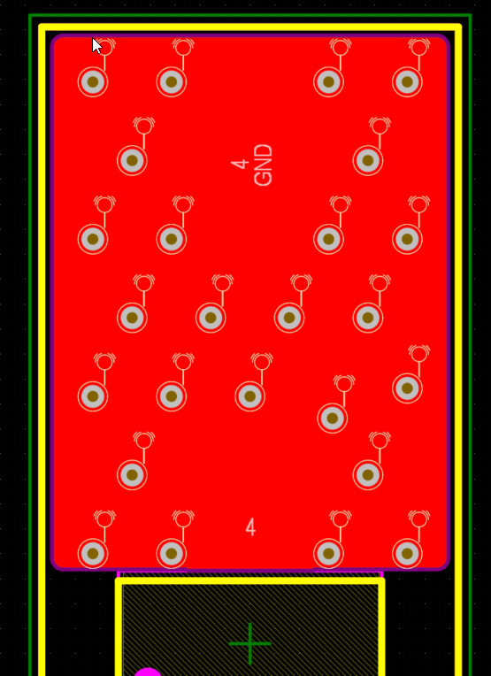
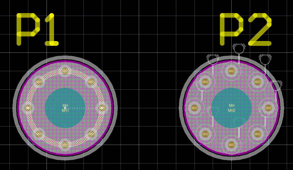
When vias are added to multilayer pads—such as thermal pads for heat dissipation or mounting holes with vias in the annular ring—Altium Designer may throw a net antenna violation. This occurs even though the vias are visibly and electrically connected to the multilayer pad.
Why This Happens
The violation is triggered because the connection between the via and the multilayer pad may not be recognized across all internal layers, especially if there is no copper region to complete the connection. This leads the design rule check (DRC) to interpret the via as an unconnected stub, resulting in a net antenna error.
Example situations include: Thermal Pad with the Through hole Via or Multilayer Through Hole Pad with the Via
What to Do
There are three possible solutions:
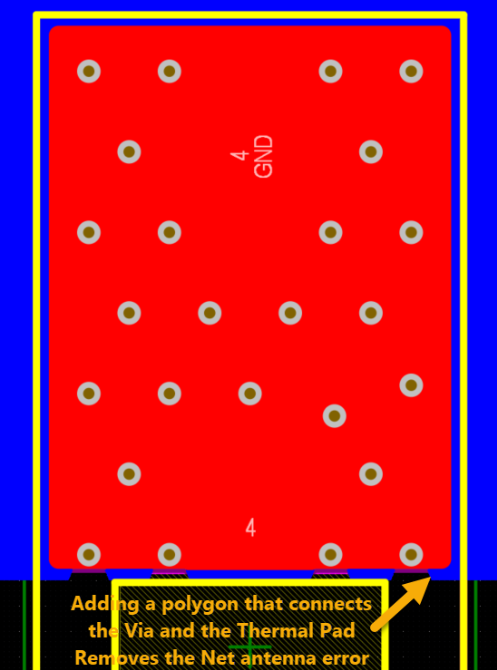
- Solution 1: Add a polygon region in an internal layer to match the multilayer pad and ensure connectivity.
- Solution 2: Create a custom Net Antenna rule to exclude specific vias from triggering violations.
- Solution 3: Waive the violation with a documented note.
How to Do It
Solution 1: Add Polygon Region
- Open the internal layer where the multilayer pad is present.
- Add a polygon region that overlaps the pad and vias.
- Ensure the polygon is assigned to the correct net.
- Re-run the DRC to confirm the violation is resolved.
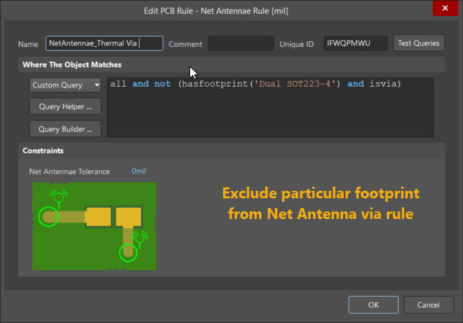
Solution 2: Create a Custom Net Antenna Rule
- Open the PCB Rules and Constraints dialog.
- Navigate to Electrical » Net Antenna.
- Create a new rule with a custom scope, e.g.:
All and not (HasFootprint('FootprintName') and IsVia) - Apply the rule and re-run the DRC.
Solution 3: Waive the Violation
- Right-click on the violation in the Messages panel.
- Select Waive Violation.
- Add a note explaining the reason for the waiver.
- Refer to Altium’s documentation on waiving DRC violations: Selectively Waiving DRC Violations
- Always verify that the vias are electrically connected across all relevant layers.
- Use waivers only when the design intent is clear and documented.
- Custom rules should be tested to ensure they do not unintentionally suppress valid violations.