
KB: Draftsman Fabrication View Shows Only Part of PCB in Altium Designer
Updated: May 28, 2026
 Altium Designer
In Altium Designer, a Draftsman Fabrication View may display only part of the PCB, such as a single quadrant, even though the full board is visible in the PCB Editor. This typically occurs when a Route Tool Path Outline exists in the PCB document and Draftsman interprets it as the board boundary. As a result, any copper or board area outside that boundary is hidden. This behavior is controlled on a per-view basis. Enabling Show Out of Board Copper in the affected Fabrication View restores visibility of the full PCB. For panelization workflows, placing route tool paths in a dedicated panel PCB document and using that panel as the Draftsman data source prevents unintended view cropping.
Solution Details
Only part of the board appears
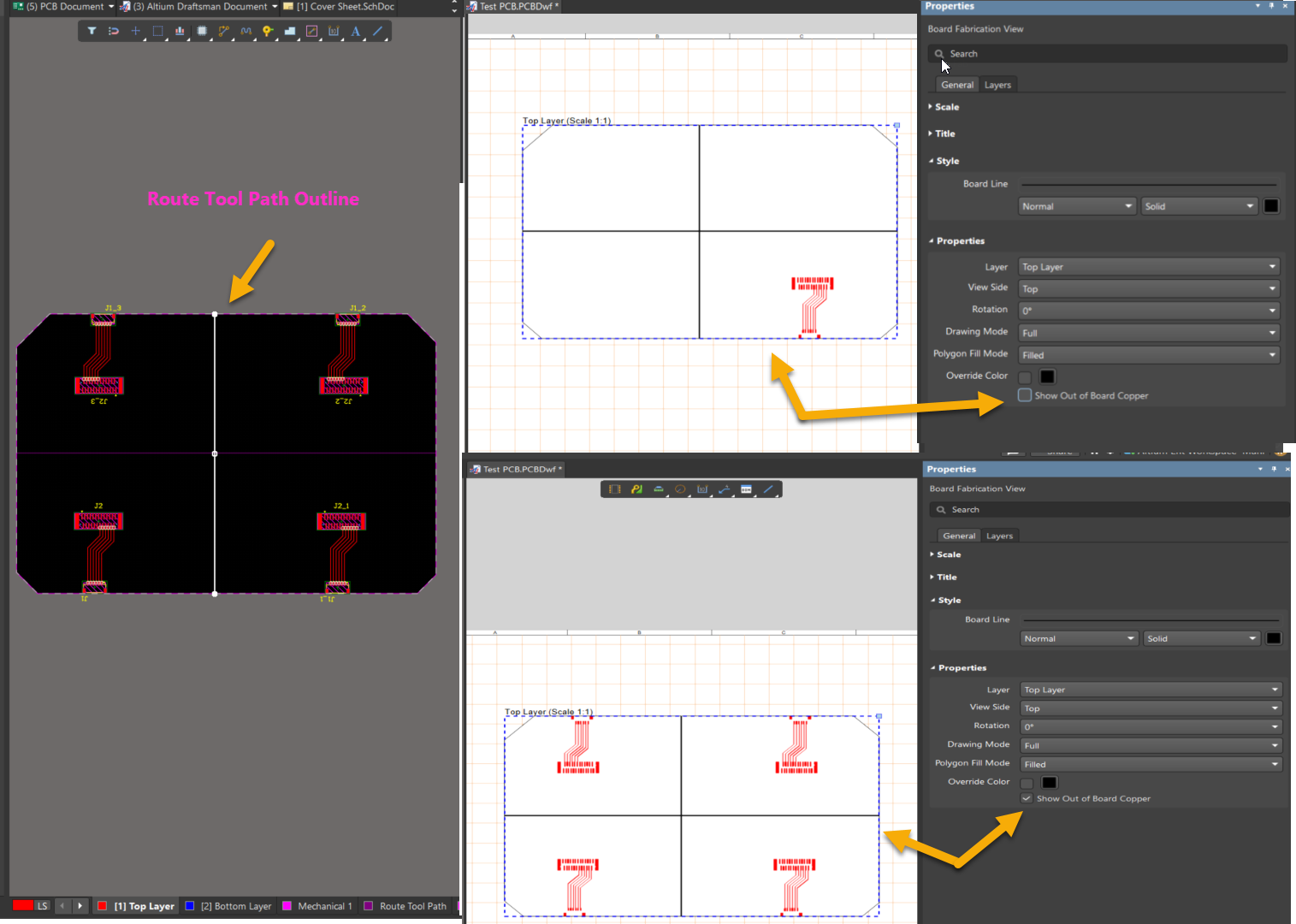
In the Draftsman Fabrication View, only a section of the PCB is shown while other areas are missing. The same PCB displays correctly in the PCB Editor. This behavior is consistent across both older and current versions of Altium Designer.
Route Tool Path defines view boundary
A Route Tool Path Outline exists in the PCB document, typically drawn on a mechanical layer nominated as the Route Tool Path layer. Draftsman treats this outline as the effective board boundary for the selected Fabrication View. Any copper or board area outside this boundary is hidden unless explicitly configured to be shown. Rendering behavior and boundary interpretation are controlled per placed view, not globally for the Draftsman document.
Enable copper visibility or change data source
- Enable Show Out of Board Copper in the selected Fabrication View to display all board areas.
- If the Route Tool Path is intended for panelization, move it to a dedicated panel PCB document and use that panel PCB as the Draftsman data source.
Configure the view
- Open the Draftsman document (
*.PCBDwf). - Select the Fabrication View that shows only a partial PCB.
- Open the Properties panel via Panels » Properties.
- In the General » Properties section for the selected Fabrication View, enable Show Out of Board Copper.
- Verify that all PCB areas are now visible and match the PCB Editor.
Recommended workflow when using Route Tool Path
- Create a panel PCB document via File » New » PCB.
- Insert the PCB into the panel using Place » Embedded Board Array/Panelize.
- Draw the Route Tool Path only in the panel PCB document, not in the single‑PCB file.
- Select the panel PCB as the Draftsman data source using one of the following methods:
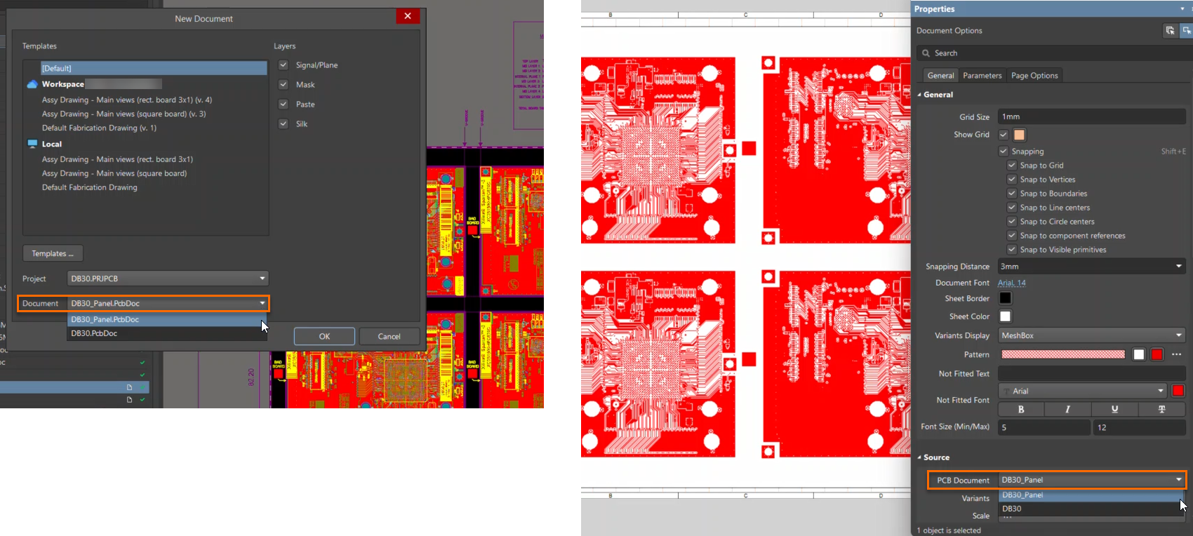
- When creating a new Draftsman document, select the panel PCB in the New Document dialog.
- For an existing Draftsman document, deselect all objects to access the Document Options in the Properties panel, then select the PCB document under Source.
- Place a new Fabrication View using the panel PCB as the source.
Additional Notes
- After enabling Show Out of Board Copper, ensure all quadrants of the PCB are visible.
- Confirm the Route Tool Path Outline no longer restricts the view.
- Cross-check the Draftsman view with the PCB Editor for visual consistency.
- Fabrication-related geometry such as panel outlines, breakaway tabs, and route tool paths should reside in the panel PCB to avoid unintended cropping.